Degroot.pdf
This document was uploaded by user and they confirmed that they have the permission to share it. If you are author or own the copyright of this book, please report to us by using this DMCA report form. Report DMCA
Overview
Download & View Degroot.pdf as PDF for free.
More details
- Words: 30,985
- Pages: 93
1
PHYS3004 Crystalline Solids Dr James Bateman
Course notes created by Prof. P.A.J. de Groot and adopted with thanks for use in the 2012/2013 academic session
James Bateman Course Co-ordinator, PHYS 3004 [email protected]
2
Introduction These course notes, the creation of Prof. Peter de Groot, define the content that I shall deliver for the Level 3 core module on Crystalline Solids. Supplementary material, including various problem sheets, adopted with thanks from Prof. Anne Tropper. The course consists of 30 teaching sessions, delivered in Semester I. New material will be taught each week in a double lecture slot on Tuesday, 9:00 – 11:00, in Building 2 Room 1089. The single lecture each Thursday, 17:00 – 18:00, also in 02/1089, will be devoted to problem solving, based partly on problem sheets and partly on past exam papers. Students are strongly advised to work through all problem sheets before this lecture; independent study is crucial at this stage in your career. There will be no correction or assessment of written work but there will be ample opportunity for students to ask questions in the Thursday lectures. The first lecture is scheduled for Tuesday 2nd October in week 1. Six hours per week of independent study is expected of students. Assessment is by 2-hour written examination at the end of the course. The examination paper contains two sections. Section A (40 minutes) is compulsory and consists of short questions taken from all parts of the course. Section B contains 4 longer questions, from which candidates must answer 2 (40 minutes each). The recommended course book is “Introductory Solid State Physics” by H.P. Myers (£45.59 paperback edition from Amazon). There are many other excellent texts on this subject, mostly somewhat more advanced. These include: “Solid State Physics” by N.W. Ashcroft and N.D. Mermin (Thomson Learning). “Introduction to Solid State Physics” by C. Kittel (J. Wiley) The original text from 1953, now in its 7th edition (1996). Mathematically thorough; be sure to read the preface as the chapter order assumes no QM knowledge.
“Solid State Physics” by J.R. Hook and H.E Hall (Wiley) This covers most of the course material at the right level, but makes no mention of optical properties of solids or their applications.
“Optical properties of solids” M. Fox (OUP) This treats optical properties with quite some breadth. Qualitative approach to QM combined with classical EM. Wide ranging and easy to follow. recommendations above with thanks to Prof. Chris Phillips
Course materials will be downloadable from the course website at http://www.phys.soton.ac.uk/module-list James Bateman [email protected] 2nd October 2012
3
1. Bonding in Solids (Assumes knowledge of atoms and classical thermodynamics) Suggested reading Myers Chapter 1 pages 20-28.
1.1 Introduction Solids in general, and in particular crystalline solids, are characterized by a very orderly arrangement of atoms. In the case of crystalline solids the lattice has full translational symmetry at least, i.e. if the crystal is moved in any direction by a lattice vector it looks/is the same as before it was moved. Thus the solid state has very little entropy (is very ordered and thus “unlikely”). Why therefore do solids form? Thermodynamics tells us that if the system’s entropy has to decrease to form a solid the system has to give energy to the surroundings otherwise solids would not form. From this experimental evidence we can deduce that solids form because atoms and molecules exert attractive forces on each other. These attractive forces between atoms/molecules in solids are called bonds. However we know by measuring the density of a wide range of materials that although atoms are mostly made up of empty space there is a limit to how close they will pack together. That is, at some equilibrium distance the forces of attraction between atoms become zero and for distances closer than that the atoms repel. One way of representing this is to consider the potential energy that two atoms have due to each other at different distances. A generic form of this is given in the diagram below. The zero of potential energy is chosen to be when the atoms are infinitely far apart. As force is equal to the gradient of potential energy it is clear that the equilibrium separation will be at the minimum of the potential energy. We can also read off from the graph the energy required to separate the atoms to infinity, the binding energy.
Equilibrium Seperation
1.0
Potential Energy (arb. units)
Attractive Interaction
Repulsive Interaction
0.5
0.0 Binding Energy
-0.5 2.5
3.0
3.5
4.0
4.5
5.0
5.5
6.0
Seperation of Atoms (nm)
Figure 1.1: A schematic representation of the interaction potential energy between two atoms.
4
One thing that is easily observed is that different materials crystallize at different temperatures. We know from thermodynamics that the temperature at which crystallization occurs, the melting or sublimation temperature, is when the entropy decrease of the material on crystallizing is equal to the energy given out due to crystallization divided by the temperature; ∆S = ∆E / T . Therefore the melting/sublimation temperature provides us with our first piece of evidence about bonds in solids with which to build our theories. Materials with high melting/sublimation temperatures give out more energy when the bonds are formed i.e. they have stronger bonds. However as crystals often form from liquids, in which the atoms or molecules are relatively close and therefore still interacting, the melting/sublimation temperature isn’t a perfect measure of the energy stored in the bonds. Table 1.1 Melting/sublimation temperature for a number of different solids. Substance
Melting/Sublimation Temperature (K)
Argon
84
Nitrogen
63
Water
273
Carbon dioxide
216 – sublimation
Methanol
179
Gold
1337
Salt (NaCl)
1074
Silicon
1683
From Table 1.1 we can see that there is a huge range of melting/sublimation temperatures. This strongly suggests that the there must be more than one type of bond in solids, i.e. the forces between argon atoms and between silicon atoms are quite different. What other experimental evidence is available to us to help us understand bonding? Well one obvious thing we could try and do is measure the forces on the atoms by compressing or stretching a material and measuring its elastic constants. Such measurements do indeed show that silicon is much stiffer than ice, as expected from the stronger bonds in silicon, however these mechanical properties of a material often strongly depend on the history of the sample and defects within the sample, and are not simple to understand. In x-ray diffraction, which will be described in more detail in later sections, xray photons are being scattered from the electrons in a solid. In fact, x-ray diffraction allows us to map out the electron density within solids i.e. the maps of the probability of finding an electron at a certain place within the crystal. Two such maps, for
5 diamond and NaCl, are shown below. These maps show that most of the electrons in the solid are still held quite close to the nuclei of the atoms; the electron density is much higher nearer the center of the atoms. In addition they show that the orbitals of these electrons are not much disturbed from their positions in atoms in a dilute gas, i.e. they are still spherical. These electrons are often called the core electrons. However in both NaCl and diamond not all the electrons are undisturbed in the solid compared to the gas. In the case of NaCl the x-ray diffraction shows that one electron has mostly transferred from the Na atom to the Cl atom forming Na+ and Cl- ions; this can be seen by integrating the electron density over a sphere centered on each ion to determine the number of electron associated with each atom. In the case of diamond it appears that some of the electrons from each carbon, actually 4 electrons from each carbon (one for each of it’s neighboring carbons), can now be found between the carbon atoms as if they were now being shared between neighboring carbon atoms. This can be seen from the fact that the electron density between atoms A and B is no lower than 5 however in the areas away from the atoms the electron density drops to 0.34. From these observations we can deduce that although most of the electrons, the core electrons, of an atom are relatively undisturbed in a crystal some of the electrons are quite strongly disturbed.
Figure 1.2: (a) X-ray diffraction map of electron density for diamond. The lines are contours of constant electron density and are numbered with their electron density. (b) unit cell of diamond. The gray plane corresponds to the electron density map above, as do the labeled atoms. (c) electron density map for NaCl for plane through one face of the cubic unit cell (d).
6
We have now gathered quite a lot of information about how solids are bound together and so we will now discuss qualitatively some of the theories that have been developed to understand the process of bonding in solids. Before we go on to discuss the various standard bonding models we first need to answer a very general question. Which of the fundamental forces of nature is responsible for bonding in solids? The answer is the electromagnetic force. Gravity is too weak and the nuclear forces are too short range. The general form of the attraction is shown in the schematic below. The basic concept is that when two atoms are brought together the nuclei of one atom is electromagnetically attracted to the electrons of the other atom. For bonding to occur the total attraction between electrons and nuclei has to be stronger than the repulsion due to the electron-electron and nuclei-nuclei interactions. Although in many cases these attractions are not discussed explicitly this is the underlying mechanism behind all the different forms of bonding in solids.
+
+ -
Figure 1.3: Two hydrogen atoms in close proximity showing the electromagnetic interactions between the two nuclei and two electrons. The solid lines denote attractive interactions, the broken lines repulsive interactions.
1.2 Covalent Bonding Covalent bonding is so named because it involves the sharing of electrons between different atoms with the electrons becoming delocalised over at least two atoms. It is an extremely important form of bonding because it is responsible for the majority of bonding in all organic molecules (carbon based) including nearly all biologically important molecules. In order to try and understand covalent bonding let us first look at covalent bonding in the simplest possible molecule H2+ i.e. two protons and one electron. It is clear that if we separate the two nuclei very far apart then the electron will be associated with one nuclei or the other and that if we could force the two nuclei very close together then the electron would orbit the two nuclei as if they were a helium nucleus. What happens for intermediate separations? To answer this we need to solve Schrodinger’s wave equations for the electron and two nuclei. This equation contains terms for the kinetic energy of the electron and the two nuclei and all the electrostatic interactions between the three particles. It is in fact impossible to solve this problem analytically as it involves more than two bodies. Therefore we need to make an approximation to make the problem solvable. The standard approximation is called the Born-Oppenheimer approximation and it is based on the fact that the electron is 2000 times less massive than a proton. This means that a proton with the same kinetic energy as an electron is moving roughly 50 times slower than the electron. The Born-Oppenheimer approximation states that as far as the
7 electron is concerned the protons (nuclei) are stationary. We then solve the Schrodinger equation for the electron to obtain the eigenstates (orbitals) and their energies. The groundstate and first excited state electron orbitals obtained from such a calculation for different nuclear separations are shown in Fig. 1.4. The energy of these orbitals as a function of nuclear separation is also shown in Fig. 1.4. We can see from the latter figure that only the lowest energy orbital gives a lower energy than infinitely separated atoms and thus only if the electron is in this orbital will the nuclei stay bound together. For this reason this orbital is called a bonding orbital whereas the first excited state is called an anti-bonding orbital.
Figure 1.4: Electron density maps for (a) the lowest energy (bonding) and (b) the first excited (anti-bonding) electron orbitals of the molecule H2+ at different fixed (Born-Oppenheimer Approximation) nuclear separations R. The graph on the far right is the energy of the molecule as a function of nuclear separation for the bonding and anti-bonding orbitals.
What causes the difference between the two states? This can be clearly seen when we examine the electron density along the line joining the two nuclei and compare them against the electrostatic potential energy of the electron due to the two nuclei along the same line. The bonding orbital concentrates electron density between the nuclei where the electrostatic potential energy is most negative. Where as, the anti-bonding orbital has a node half way between the nuclei and it’s electron density is mostly outside the region where the electrostatic potential energy is most negative.
8
Orbitals (Electron Density) Bonding Orbital Anti-bonding Orbital
Electrostatic Potential
Figure 1.5: Comparison of Bonding and Anti-Bonding orbitals against the electrostatic potential due to the two nuclei. From Fig.1.5 we can see that even if the electron is in the bonding orbital that the molecule’s energy has a minimum for a finite separation and then increases for smaller separation. From the calculations we can show that for this molecule this is mostly because of the electrostatic repulsion between the nuclei however as we will discuss later other effects can be important in bonds between atoms with many electrons.
√2 Ψ1 +Ψbonding Ψ2 = (ψ = 1 + ψΨ 2) /bonding
) / √2 Ψ1 −Ψanti-bonding Ψ2 == (ψ1 -Ψψ2anti-bonding
Figure 1.6: Schematic representation of the Linear Combination of Atomic Orbitals. The bonding orbital is produced by constructive interference of the wavefunctions in the area between the nuclei and the anti-bonding orbital by destructive interference. Even with the Born-Oppenheimer approximation solving for the orbitals of the H2 is complicated and so often we make another approximation which is based on the fact that the true molecular orbitals shown above are well approximated by a sum of two atomic 1S orbitals, one on each atom. This is shown schematically in Fig.1.6. +
9 This approximation, that the molecular orbitals can be made from the sum of atomic orbitals, is called the linear combination of atomic orbitalsi. So far we have only treated the simplest of molecules. How do we treat molecules with more than one electron? Well we go about this in a similar manner to how we treat atoms with more than one electron. That is we take the orbitals calculated for a single electron and add electrons one by one taking into account the Pauli exclusion principle. So what happens with H2 the next most complicated molecule. Well the two electrons can both go into the bonding orbital and H2 is a stable molecule. What about He2? Well we have 4 electrons, 2 go into the bonding orbital and 2 into the anti-bonding orbital. In fact it turns out that the anti-bonding orbital’s energy is greater than two separate atoms by more than the bonding orbital is less than two separate atoms and so the whole molecule is unstable and does not exist in nature. What about Li2 ii in this case we have 6 electrons the first four go as in He2 and are core electrons. The contribution of these electrons to the total energy of the molecule is positive and leads to a repulsion between the nuclei. For bonding between atoms with more than one electron each, this repulsion adds to the repulsion due to the electrostatic repulsion between nuclei to give the repulsion that keep the atoms from coming too close. The final two electrons go into the bonding orbital formed from the two 2S atomic orbitals. These electrons make a negative contribution to the molecules total energy large enough that Li2 would be stable. As the 2S orbitals extend further from the nuclei than 1S and the core electrons lead to a repulsive interaction between the nuclei the equilibrium nuclear separation will be relatively large compared with the 1S orbitals. We know from the calculations of molecular orbitals that this means the core orbitals will be very similar to separate 1S orbitals. Which explains why core electrons do not seem to be disturbed much by bonding. So far I have only talked about molecular orbitals formed from linear combinations of S symmetry atomic orbitals however of course it is possible to form covalent bonds from P, D and all the other atomic orbitals. As the P and D orbitals can be thought of as pointing in a certain direction from the atom (Fig. 1.7). It is these orbitals that produce the directionality in covalent bonding that leads to the very non close packed structure of many covalent solids such as diamond. However this subject is more complex and I will not deal with it explicitly. If you are interested I suggest you read more in a basic chemistry textbook like Atkins (Chapter 10).
Figure 1.7: Constant electron density surface maps of S, P and D atomic orbitals. i
In fact the method is only approximate because we are only using one atomic orbital for each nuclei. If we were to use all of the possible orbitals the method would be exact. ii Of course lithium is a metal and doesn’t naturally form diatomic molecules.
10 I have also only discussed covalent bonding between identical atoms. If the two atoms are not identical then instead of the electrons in the bond being shared equally between the two atoms the electrons in the bonding orbitals will spend more time on one of the atoms and those in the anti-bonding orbital on the other atom. However for atoms that are fairly similar like carbon, oxygen, sulphur etc. the split of the electrons between the two atoms is fairly equal and the bonds are still mostly covalent in nature. If the atoms are very different like Na and Cl then we have instead ionic bonding.
1.3 Ionic Bonding When discussing covalent bonds between two different atoms I talked about similar and different. These are not very specific terms. Why are carbon and sulphur similar and sodium and chlorine different. In terms of ionic and covalent bonding there are two energies that are important for determining whether the atoms form an ionic or covalent bondiii. These are the electron affinity, the energy difference between a charge neutral atom or negative ion with and without an extra electron (e.g. O → O), and the ionization energy, the energy required to remove an electron from the a charge neutral atom or positive ion, (e.g. O → O+). In Table 1.2 we present these energies for the series of atoms Li to Ne. It is left to the reader to think about why the series show the trends that they do. Table 1.2 : Electron affinities and first ionisation energies for the second row of the periodic table. Element Lithium
First Ionization Energy (eV/atom) 5.4
Electron Affinity (eV/atom) -0.62
Beryllium
9.3
No stable negative ions
Boron
8.3
-0.28
Carbon
11.2
-1.27
Nitrogen
14.5
0
Oxygen
13.6
-1.43
Fluorine
17.4
-3.41
Neon
21.5
No stable negative ions
iii
Note that although pure covalent bonds can occur between two identical atoms pure ionic bonding is not possible as the electrons on a negative ion will always be attracted to towards positive ions and therefore be more likely to be found in the volume between the ions i.e. be shared. Thus ionic and covalent bonds should be considered ideals at either end of an experimentally observed continuum.
11 Now imagine we were to remove an electron from a carbon atom and give it to another carbon atom the total energy required to make this change is 11.2 –1.27 = 10eV/atom. However if we were instead to take an electron from a lithium atom, forming a Li+ ion, and give it to a fluorine atom, forming a F- ion, the total energy required would be 2 eV/atom, which is much less. The energy we have just calculated is for the case that the atoms, and ions which form from them, are infinitely far apart. However if we were to bring the ions together then the total energy of the system would be lowered. For a Li+ and F- ions 0.35 nm apart, the separation in a LiF crystal, the electrostatic potential energy would be 4 eV. Of course in a LiF crystal the Li+ ions don’t interact with a single F- but with all the other ions in the crystal, both Li+ and F-. When all of these interactions are taken into consideration the magnitude of the electrostatic potential energy of the crystal is much larger than the energy cost for forming the ions and therefore the crystal is stable. This type of bonding where electrons transfer to form ions that are electrostatically bound is called ionic bondingiv. We have only discussed the transfer of one electron between atoms however a large number of ionic crystals do exist with ions with more than one excess or removed electron. For instance it is relatively easy, i.e. low energy cost, to remove two electrons from group II atoms and group VI atoms will easily accept two electrons. Also there are a number of ions that are made up of more than one atom covalently bound, for instance CO32-.
1.4 Metallic Bonding This bonding is in many ways similar to the covalent bond in as much as the electrons are shared amongst the atoms. It’s main difference is that in this type of bonding the electrons are not localized in the region between atoms but instead are delocalised over the whole crystal. Another way of looking at metallic bonding is that every atom in the metal gives up one or more electrons to become a positive ion and that these ions are sitting in a “sea” or “cloud” of free electrons. The atoms stay bound because the electrostatic interaction of the electrons with the ions. +
+
+
+
+
+
+
+
+
+
+
+
+
+
+
+
+
+
+
+
+
+
+
+
+
+
+
+
+
+
+
+
+
+
+
Metallic Elec tron “Cloud” Ion
Figure 1.8: Schematic representation of a metallically bonded material. Charged ions surrounded by a "cloud" or "sea" of delocalised electrons.
iv
In fact pure ionic bonds do not exist, unlike pure covalent bonds, as the electrons around any negative ions are attracted to it’s positive neighbors they are more often found between the ions and all ionic bonds have a very small covalent component.
12 Now is a convenient time to stress that the bonding models we have been discussing are theoretical concepts and that often in real materials the bonding is a mixture of a number of different models. A good example of this is the way that it is possible to describe the metallic bond as being like a covalent and an ionic bond. The key to understanding metallic bonding is that the electrons are delocalised.
1.5 Van der Waals Bonding When discussing covalent bonding we stated that He2 is not stable and for the same reason we would not expect Ar2 to be stable, however Argon does crystallize. What is the bonding mechanism in this case. It can’t be ionic as we don’t have two types of atoms. We also know that solid argon is not metallicv. In fact it turns out that in solid argon the bonding mechanism is a new type called van der Waal’s bonding. Argon atoms, like all atoms, consist of a positive nucleus with electrons orbiting it. Whenever an electron is not at the center of the nucleus, it and the nucleus form a charge dipole. Now as the electron is constantly moving the average dipole due to the electron and nucleus is zerovi. However let us consider an atom frozen in time when the electron and nucleus form a charge dipole p1. Well a charge dipole produces an electric field, E, of magnitude proportional to p1. This electric field can electrically polarize neighboring atoms, i.e. cause them to become dipoles aligned parallel to the electric field due to the first atom’s dipole. The magnitude of the dipole in the second atom, p2, will be proportional to the electric field, E. Now a dipole in the presence of an electric field has an electrostatic energy associated with it given by p.E. Thus, the dipole at the second atom will therefore have an energy due to being in the presence of the electric field due to the first atoms dipole as p // E. As p = αE the energy of the second dipole due to the first is proportional is the magnitude of the first dipole squared i.e. α|p1|2. Now although the average, over time, of the first atoms dipole is zero the interaction energy we have just derived does not depend on the direction of the dipole of the first atom therefore it will not average to zero over time. This fluctuating dipole- fluctuating dipole interaction between atoms is the van der Waal’s interaction. From the fact that the electric field due to a dipole falls off as 1/r3 we can deduce that the van der Waal’s interaction falls off as 1/r6.
1.6 Hydrogen Bonding Hydrogen bonding is extremely important for biological systems and is necessary for life to exist. It is also responsible for the unusual properties of water. It is of intermediate strength between covalent and van der Waals bonding. It occurs between molecules that have hydrogen atoms bonded to atoms, such as oxygen, nitrogen and chlorine, which have large electron affinities. Hydrogen bonding is due to the fact that in the covalent bond between the hydrogen and the other atom the electrons reside mostly on the other atom due to its strong electron affinity (see Fig. 1.9). This leads to a large static electric dipole associated with the bond and this will attract other static dipoles as set out above for van der Waals bonding. v vi
At least not at atmospheric pressure. Assuming the atom is not in an external electric field
13
Figure 1.9: Model of hydrogen bond forming between two permanent dipoles.
14
2. Crystal Lattices For additional material see Myers Chapter 2. Although some materials are disordered, many can be understood from the fact that the atoms are periodically arranged. So instead of thinking about ~1023 atoms we can think about two or three, together with the underlying symmetry of the crystal. We are going to ignore for the moment that crystals are not infinite and they have defects in them, because we can add these back in later. The first thing we notice is that crystals come in many different forms, reflecting different arrangements of the atoms. For instance:
(i)
(ii)
(iii)
Figure 2.1: Three common crystal structures; (i) face centered cubic [calcium, silver, gold] {filling fraction 0.74}, (ii) body centered cubic [lithium, molybdenum] {filling fraction 0.68} and (ii) diamond [diamond, silicon, germanium] {filling fraction 0.34}. If as a starting assumption we assume that solids are made up of the basic blocks, atoms or molecules, which are treated as incompressible spheres, stacked up to form a solid and that the attraction between the units is isotropicvii we should be able to determine how the units should be arranged by determining the arrangement which gives the largest energy of crystallization. It is obvious that what we want to do is to obtain the arrangement of the atoms that minimizes the separation between atoms and therefore the space not filled up by atoms. Such a structure is called close packed. The filling fraction is the ratio of the volume of the atoms in a crystal to the volume of the crystal. The filling fractions for the structures in Figure 2.1 are given in the caption in {} brackets. It is clear from this that many crystals don’t form in a structure that minimizes the empty space in the unit cell i.e. they are not close packed. This leads us to review our assumptions as clearly one is incorrect. In fact it turns out that in some materials the attraction between units is directional. Isotropic/directional is one important way of differentiating between bonding in different materials. In this course we are not going to attempt any sort of exhaustive survey of crystal structures. The reason is that there are an incredible number although they can be fairly well classified into different ‘classes’. What we will do is introduce a formalism because it will help to view the diffraction of lattices in a powerful way, which will eventually help us understand how electrons move around inside the lattices.
vii
Isotropic – the same in all directions.
15 The first part of our formalism is to divide the structure up into the lattice and the basis. The lattice is an infinite array of points in space arranged so that each point has identical surroundings. In other words, you can go to any lattice point and it will have the same environment as any other. Nearest-neighbour lattice points are separated from each other by the 3 fundamental translation vectors of the particular 3dimensional (3D) lattice, which we generally write as a, b and c. Then any lattice points are linked by a lattice vector: R = n1 a + n2 b + n3 c (where n1, n2, n3 are integers). An example in 2D:
R1
Fig. 2.1a Simple 2D lattice structure Here R1 = 2a + b = 3a’ + b’ is a lattice vector. The basis of the crystal is just the specific arrangement of atoms attached to each lattice point. So for instance we can have a three atom basis attached to the above lattice to give the crystal structure:
RT11 X
Fig. 2.1b Simple 2D lattice structure with basis. Moving by any lattice vector (e.g. R1) goes to a position which looks identical. This reflects the translational symmetry of the crystal. Note that X is not a lattice vector, as the shift it produces results in a different atomic environment. Most elements have a small number of atoms in the basis; for instance silicon has two.
16 However α-Mn has a basis with 29 atoms! Compounds must have a basis with more than one atom, e.g. CaF2 has one Ca atom and two F atoms in its basis. Molecular crystals (such as proteins) have a large molecule as each basis, and this basis is often what is of interest – i.e. it is the structure of each molecule that is wanted. We often talk about the primitive cell of a lattice, which is the volume associated with a single lattice point. You can find the primitive cell using the following procedure: (i) (ii) (iii)
Draw in all lattice vectors from one lattice point, Construct all planes which divide the vectors in half at right angles, Find the volume around the lattice point enclosed by these planes.
(i)
(ii) (iii)
a)
b)
Fig. 2.2: Construction of the Wigner-Seitz cell ( a), other primitive cells (b). This type of primitive cell is called a Wigner-Seitz cell, but other ones are possible with the same volume (or area in this 2D case), and which can be tiled to fill up all of space. On the basis of symmetry, we can catalog lattices into a finite number of different types (‘Bravais’ lattices): 5 in 2 dimensions 14 in 3 dimensions Each of these has a particular set of rotation and mirror symmetry axes. The least symmetrical 3D lattice is called triclinic, with the fundamental vectors a, b and c of different lengths and at different angles to each other. The most symmetrical is the cubic, with |a|=|b|=|c| all at right-angles.
17 In this course we will often use examples of the cubic type which has three common but different varieties: simple cubic, body-centered cubic (bcc) and facecentered cubic (fcc). The latter two are formed by adding extra lattice points to the unit cell either in the center of the cell, or at the center of each face. The cubic unit cell is then no longer primitive, but is still most convenient to work with. Now we are in a position to extend our formalism further:
Positions in the unit cell are defined in terms of the cubic “basis” vectors a, b, c. The position ua+vb+wc is described uvw. Only in the cubic system are these like Cartesian coordinates. For example, for the • simple cubic lattice there is just one atom at 000 • body centre cubic lattice (bcc) the atomic positions are 000, 1/21/21/2 • face centre cubic lattice (fcc) the atomic positions are 000, 01/21/2, 1/201/2, 1 1 /2 /20 Directions in the crystal are defined by integer multiples of the fundamental vectors. The direction of the vector ua+vb+wc is described [uvw]. So the body diagonal direction is [111]. Negative components are written with a bar above the number instead of a confusing minus sign, e.g. 1 1 0 is a face diagonal.
[ ]
Planes are labelled as (uvw) – i.e. with round brackets – denoting all the lattice planes orthogonal to a direction [uvw] in the lattice. Planes in the crystal are important determining the diffraction that can occur. Although Bragg diffraction can be described in terms of the separation of different crystal planes, it is important to note that there are rather a lot of planes in even a simple sample crystal (Fig 2.3). Conversely using x-ray diffraction to measure all the spacings allowed by Braggs law does not easily allow you to work back to find the crystal structure itself. You can see this just by trying to draw the planes present in a cubic lattice:
Fig. 2.3: Selected planes in the cubic lattice This problem becomes much more difficult when we understand that virtually no material has the simple cubic lattice, but have more complicated atomic arrangements. In order to interpret diffraction patterns and understand crystal structures a concept called the “reciprocal lattice” is used which is described in the next section.
18
3. The Reciprocal Lattice For additional material see Myers Chapter 3
3.1 Diffraction of Waves from Crystals In an x-ray diffraction experiment we illuminate a sample with x-rays from a specific direction, i.e. the x-rays are a plane wave, and then measure the intensity of x-rays diffracted into all the other directions. The reason that the crystal causes the x-rays to diffract is that the x-rays electromagnetic field makes the electrons within the material oscillate. The oscillating electrons then re-emit x-rays as a point source into all directions (i.e. Huygens principle in optics). As the phase of the oscillation of all the electrons are set by a single incoming wave the emission from all the electrons interferes to produce a diffraction pattern rather than just a uniform scattering into all directions equally. We will now use Huygens’ Principle to calculate the diffraction pattern one would expect from a crystal. Let’s start with a lattice of single electrons (see fig below).
dn θ
Rn
Zero Phase
As we always have to talk about a relative phase difference we start by defining the phase at one of the electrons to be zero phase. From the diagram we can see that the phase at the electron at position Rn is given by 2πd n λ . Standard trigonometry gives
that dn is equal to Rncosθ i.e. that the relative phase is 2πRn cosθ λ . This expression is more commonly written k in .R n which is the dot product of the position of the atom and the wavevector of the x-rays. In addition to the different phase of the oscillations of the different electrons we have to take into account the different paths for the emitted x-rays to travel to the detector (see fig. below).
19
dn θ
Rn
Zero Phase
If we set the phase, at the detector, of the x-rays emitted by the zero phase electron to be zero then the phase, at the detector, of the x-rays emitted by the atom at Rn will be − 2πd n λ = − k out .R n . Thus the total phase difference of light scattered from the incoming wave at the detector by the atom at Rn will be (k in − k out ).R n and the total electric field at the detector will be proportional to:
Edet ∝ ∑ ei (k in − k out ). R n n
We know that in a real crystal the electrons are not localized and instead should be described by a electron density function, e.g. ρ e (r ) . In this realistic case the expression is given by
Edet ∝
i ( k in − k out ).r ( ) ρ r e dV ∫∫∫ e
crystal
3.2 The Effect of the Lattice The defining property of a crystal is that it has translational symmetry. The importance of this to x-ray diffraction is that the electron density at a point r and another point r + Rn where Rn is a lattice vector must be the same. This means that if we write the integral above as a sum of integrals over each unit cell, i.e.
Edet ∝ ∑ Rn
Edet
20
i ( k in − k out ).( r + R n ) ρ ( r + R ) e dV n ∫∫∫ e
i ( k in − k out ). R n ∫∫∫ ρe (r )ei ( k in −k out ).( r ) dV ∝ ∑e R n UnitCell UnitCell
i.e. the diffracted field has two components. The first term is a sum over the lattice vectors and the second term is due to the charge density in the unit cell. We will first investigate the effect of the first term. As Rn is a lattice vector we know it can be written in the form R n = n1 a 1 + n 2 a 2 + n3 a 3 . If we define Q = k out − k in and substitute for Rn we get
Edet ∝
∑e
= ∑e
− i Q .( n1 a 1 + n2 a 2 + n3 a )
n1 , n2 , n3
− in1 Q . a1
×∑e
n1
− in 2 Q . a 2
n2
×∑e
− in3 Q . a 3
n1
Now each of the factors in the multiplication can be represented as the sum of a series of vectors in the complex plane (Argand diagram) where the angle of the vectors relative to the real (x) axis increase from one vector in the series to the next by Q.a i . In the general case the sum can be represented by a diagram where the vectors end up curving back on themselves (as below) leading to a sum which is zero.
I
R The only time when this is not true is when the angle between vectors in the series is zero or an integer multiple of 2π. In this case all of the vectors are along a single line and the sum has magnitude equal to the number of vectors. Whilst the above is not a mathematical proof the conclusion that the scattering is only non-zero in the case that Q.a1 = 2π × integer, Q.a 2 = 2π × integer, Q.a 3 = 2π × integer can be shown to be true mathematically. From these expressions we can determine that the x-rays will only be diffracted into a finite set of directions ( Q ). We can most easily characterize each possible direction by the 3 integers in the above expression ∗ which are usually labeled h, k, l. Let us consider the vector difference a1 between the Q corresponding to h,k,l and that corresponding to h+1,k,l. This vector is defined by the equations;
21
∗
∗
∗
a1 .a 1 = 2π , a 1 .a 2 = 0, a 1 .a 3 = 0 ∗
that is a1 is a vector which is orthogonal to a 2 and a 3 and has a component in the direction of a1 which is equal to 2π a1 .
*
a2
a2
*
a1 a1 ∗
∗
If we define similar vectors a 2 and a 3 then the diffraction vector Q corresponding to the indices h, k, l is given by ∗
∗
∗
Q = ha 1 + k a 2 + l a 3
That is the set of diffraction vectors forms a lattice, i.e. a periodic array. Because the vectors magnitude is proportional to the reciprocal of the lattice spacing the vectors ∗ ∗ ∗ a1 , a 2 and a 3 are called reciprocal lattice vectors and the set of all diffraction vectors are called the reciprocal lattice.
3.3 Physical Reality of Reciprocal Lattice Vectors As the method by which the reciprocal lattice vectors are derived is very mathematical you might be tempted to think that they don’t have a physical reality in the same way that lattice vectors do. This is wrong. In fact there is a one to one correspondence between reciprocal lattice vectors and planes of identical atoms within the crystal, with the reciprocal lattice vector being the normal to its corresponding plane. The relationship between reciprocal lattice vectors and crystal planes means that if you rotate a crystal you are rotating its reciprocal lattice vectors in just the same way that you are rotating it’s lattice vectors.
3.4 Measuring Reciprocal Lattice Vectors using a Single Crystal Xray Diffractometer From the derivation set out above we know that in order to see diffraction of x-rays from a crystal the incoming and outgoing x-ray wavevectors have to satisfy the ∗ ∗ ∗ equation Q = k out − k in = h a 1 + k a 2 + l a 3 , i.e. the difference in the x-ray wavevectors before and after scattering is equal to a reciprocal lattice vector. Thus x-ray diffraction
22 allows us to measure the reciprocal lattice vectors of a crystal and from these the lattice vectors. In order to make such a measurement we need to determine the incoming and outgoing x-ray wavevectors. This is done by defining the direction of the x-rays by using slits to collimate the x-ray beam going from the x-ray source to the sample and the x-ray beam from the sample going to the detector. Note that the detector and its slits are normally mounted on a rotation stage allowing the direction
of kout to be controlled. The magnitude of kin is given by the energy of the x-rays from the source, which is normally chosen to be monochromatic. The magnitude of kin is given by the fact that as the energy of the x-rays is much higher than the energy of the excitations of the crystal x-ray scatting can basically be treated as elastic i.e. | kout| = | kin|.
By controlling the angle, 2θ, between the incoming and outgoing beams we control the magnitude of the scattering vector Q. In order to get diffraction from a specific reciprocal lattice vector we have to set this angle to a specific value. This angle is determined by the Bragg formula;
2π
λ x − rays
2 sin(θ ) = ha 1 + k a 2 + l a 3 ∗
∗
∗
However controlling 2Θ is not enough to ensure we get diffraction in addition we have to rotate the crystal so that one of it’s reciprocal lattice vectors is in the direction of Q.
23
Figure 3.1: (Left) Crystal not rotated correctly therefore no diffraction, (right) crystal rotated correctly for diffraction
For this reason in a single crystal x-ray diffractometer the sample is also mounted on a rotation stage which allows it to be rotated about 2 different axis by angles ω (omega) φ (phi) respectively. This is why single crystal diffractometers are called 3 axis diffractometers. Below is a picture of a diffractometer currently being used in Southampton.
3.5 The Effect of the Unit Cell/Basis- The Structure Factor So far we have only calculated the effect of the lattice on the diffraction pattern. What happens if we include the effect of the unit cell? As the lattice and unit cells terms are multiplied together it is clear that diffraction will only occur if the scattering vector is equal to a reciprocal lattice vector. This means that the effect of the unit cell can only be to alter the relative intensity of the scattering from different reciprocal lattice vectors. The effect of the unit cell occurs via the integral over a single unit cell which is called the structure factor:
SF =
∫∫∫ρe (r )e dV i Q.r
UnitCell
24 In order to try and understand what effect the atoms in the unit cell we will consider two simple models. In the first we will have the simplest type of unit cell, i.e. a single atom. We will treat the atom as being a point like object with all of it’s electrons at it’s nucleus. Thus the electron density in the unit cell is given by ρ e (r ) = N eδ (r ) where Ne is the number electrons the atom has and δ(r) is the dirac delta function, i.e. a big spike at the origin. The result of the integral in this case is given by
∫∫∫ N eδ (r )e
i Q .r
dV = N e
Thus for a single atom the x-rays intensity is the same for all of the reciprocal lattice vectors. Next we will investigate the effect of the unit cell consisting of two different atoms with one at the origin and the other at position (1/2,1/2,1/2) [as described in the previous section: positions of atoms with the unit cell are normally defined in terms of the lattice vectors]. In this case
1 1 1 ρ e (r ) = N e1δ (r ) + N e2δ r − a 1 − a 2 − a 3 2 2 2 and
SF =
∫∫∫ ρ (r )e
i Q.r
e
dV = N + N e 1 e
2 e
1 1 1 i Q .( a1 + a 2 + a 3 ) 2 2 2
unitcell ∗
∗
∗
as diffraction only occurs when Q = ha 1 + k a 2 + l a 3 this expression can be rewritten
SF = N e1 + N e2e iπ ( h + k + l ) If h + k + l is even then the exponential equals one and the intensity will equal
( N e1 + N e2 ) 2 . If h + k + l is odd then the exponential equals minus one and the intensity will equal ( N e − N e ) . Thus if we were to measure the intensity of the different diffraction peaks we could determine the relative number of electrons on each atom (as the number of electrons will be integers this is often enough to allow the absolute numbers to be determined). 1
2 2
Of course in reality atoms are not points but instead have a finite size, however by measuring the intensity of diffraction for different reciprocal lattice vectors it is possible to determine a lot about the electron density within the unit cell.
25
1000
I / a. u.
1 500
0 20
30
40
50
60
70
80
90
2 theta / deg ree s
Figure 3.2: Diffraction pattern from a NaCl crystal. The different peak heights are due to the fact that Na+ and Cl- don’t have the same number of electrons.
3.6 Powder Diffraction Technique As most of the possible values of the 3 angles which can be varied in a 3 axis x-ray diffractometer will give absolutely no signal and until we’ve done a diffraction experiment we probably won’t know which direction the lattice, and therefore reciprocal lattice, vectors are pointing aligning a 3 axis experiment can be very, very time consuming. To get round this problem a more common way to measure diffraction patterns is to powder the sample up. A powdered sample is effectively many, many crystals orientated at random. This means that for any orientation of the sample at least some of the small crystals will be orientated so that their reciprocal lattice vectors are pointing in the direction of the scattering vector, Q, and in this case to get diffraction it is only necessary to satisfy Bragg’s law in order to get diffraction.
3.7 Properties of Reciprocal Lattice Vectors Although we have calculated the reciprocal lattice vectors by considering diffraction of x-rays they come about due to the periodicity of the lattice and therefore they are extremely important in many different aspects of discussing waves in crystals. At this stage in the course we will look at one of them however we will return to this topic several times later on. Periodic Functions The defining property of a crystal is translational symmetry. That is if you move a crystal by a lattice vector it is indistinguishable from before you moved it. An obvious example is that the electrostatic potential produced by the nuclei of the atoms making up the sample has full translational symmetry i.e. it is periodic with the period of the
26 lattice. In addition as we will go on to show later this implies that in a crystal the charge density of the eigenstates of electrons have to have the same symmetry. Because of the way we defined the reciprocal lattice vectors all waves with a wavevector which are a reciprocal lattice vector will have the same phase at two equivalent points in any unit cell (see fig.). In fact all waves which have this property have wavevectors which are reciprocal lattice vectors. Fourier theory tells us that any function which is periodic can be represented by a sum of all the sinusoidal waves which have the property that their period is such that they have the same phase at two equivalent points in any two repeat units, i.e. unit cells. As many of the properties of a crystal are periodic in the lattice and all such periodic functions can be represented as a sum of sinusoidal waves:
m( r ) =
∑ ck reciprocal e
i k reciprocal .r
k reciprocal Reciprocal lattice vectors are extremely important to nearly all aspects of the properties of materials. Lattice Vibrations Reciprocal lattice vectors are also important when we discuss sounds waves. Normally when we discuss sound in solids we are thinking about audible frequency waves with a long wavelength and therefore small wavevector. In this case it is acceptable to treat the solid as if it was continuum and ignore the fact it is made up of discrete atoms. However actually solids are made up of atoms and therefore at the smallest scales the motion caused by the sound wave has to be described in terms of the motion of individual atoms. In this case the wavevector of the sound k tells us the phase difference between the motion of the atoms in different unit cells. i.e. if the phase of oscillation in one unit cell is defined as zero then the phase in another unit cell which is a position Rn relative to the first, where Rn is therefore a lattice vector, is given by k.R n . Now if we define a new sound wave whose wavevector is given by k + q R where q R is a reciprocal lattice vector then the phase in the second unit cell is given by k .R n + q R .R n = k .R n + 2π * Integer = k .R n . As this is truly independent of Rn the first and second sound waves are indistinguishable and in fact there is only one soundwave which is described by both wavevectors. As this is true independent of which reciprocal lattice vector is chosen there are an infinite set of wavevectors which could be used to describe any particular soundwave. In order to bring some sanity to this situation there is a convention that we only use the smallest possible wavevector out of the set. Like all other vector quantities, wavevectors can be plotted in a space and therefore the set of all possible wavevectors which represent soundwaves can be plotted as a region in this space. This space is called the 1st Brillouin zone. The 1st Brillouin zone can be easily calculated as it is the Wigner-Seitz primitive unit cell of the reciprocal lattice (see previous section). Electron Wavefunctions As we will prove later on in the course the wavefunction of an electron in a solid can be written in the form
27
ψ ( r ) = u ( r )e
i k .r
where u (r + R) = u (r ) for all lattice vectors R , i.e. that u (r ) is the same at every lattice point. If we again add a reciprocal lattice vector to the wavevector then
ψ ( r ) = u ( r )e
i ( k + q ).r
= (u (r )e
i q .r
)e i k .r = u new (r )e i k .r
i.e. we can represent all possible electron wavefunctions only using wavevectors within the 1st Brillouin zone.
28
4. Free Electron Model - Jellium For additional material see Myers Chapters 6 and 7 Our first goal will be to try and understand how electrons move through solids. Even if we assume freely mobile electrons in the solid, we can predict many specific properties. We will start from what you already know from Quantum Mechanics (PHYS2003) and from the Quantum Physics of Matter course (PHYS2024) and work with that to see what it implies about the electronic properties of materials, and in particular, metals. The model we will use is incredibly simple, and yet it is very powerful and lets us make a first step in understanding how complex behaviours come about.
4.1 Free Electron States 4.1.1 Jellium potential So our first, and most basic model will be a huge number of electrons, free to move inside a box. The box is the edges of our solid, because we know that electrons don’t fall out of materials very easily (there is a large potential barrier). This must be a wild approximation since you know that solids are actually made of atoms. Rather amazingly, we can get a long way with this approximation. We will call our basic solid ‘jellium’, since the electrons can wobble around.
E V
V=0 z
L
Fig.4.1: Jellium model potential 4.1.2 Solving free electron wavefunctions You can solve this problem using basic Quantum Mechanics: First you need the Schrödinger equation for electrons in free electron gas. −
h2 2 ∇ ψ + Vψ = Eψ 2m
(4.1)
29 We have to assume that each electron doesn’t need to know exactly where every other electron is before we can calculate its motion. There are so many electrons that each electron only feels an average from the others, and we include this in the total potential energy V. This is a particle in a box problem, which you know how to solve. First you know that the momentum of the particle is a constant of the motion, i.e. the electrons are described by plane waves. This means they just bounce backwards and forwards against each side of the box, like the waves on a string. The solution is then a plane wave:
ψ=
1 V
ei ( k.r −ωt ) =
1 V
e
i ( k x x + k y y + k z z ) − iω t
(4.2)
e
The pre-factor (V is the volume of the box) is just a normalisation constant to make sure that the probability of finding the particle inside the box is unity. Given the wavefunction isψ = Ae i ( k .r −ω t ) , then we know the electrons are all in the sample, so
∫ ψ ψ dV = A V = 1 , so
+∞
*
2
−∞
A=
1 V
The probability of electrons being in a certain volume is
∫ ψ ψ dV = dV / V . This *
implies that the probability for finding the electron just depends on the size of the volume we are considering compared to the total volume containing the electrons. So the electrons are uniformly distributed which is what the idea of plane waves would lead us to expect.
Re(ψ) 1/L
|ψ|2
x L
x
Fig. 4.2: Plane wave states have equal probability density throughout space (1D in this example)
You should also remember that the energy of these plane wave solutions is just given by their kinetic energy (the bottom of the box is at an arbitrary potential) and equals:
h2 k 2 E= 2me
(4.3)
30
Energy
ky
kx
kx
Fig 4.3: (a) Dispersion relation of Jellium
(b) Constant energy contour in k-space
This result is not particularly surprising since we have that the energy ~ k2, which is just the kinetic energy of a free particle (momentum hk = mv and E = mv 2 / 2 ). We have drawn here (Fig.4.3) the energy of the electrons as a function of their momentum, a dependence called their ‘dispersion relation’. This concept is pervasive throughout all physics because the dispersion relation dependence gives you a strong indication of how the waves or particles that it describes will behave in different conditions. For instance, if the dispersion relation is quadratic (as here) it gives us the feeling that the electrons are behaving roughly like billiard balls which are well described by their kinetic energy. In other cases you will see a dispersion relation which is extremely deformed from this (later in the course) in which case you know there are other interactions having an effect, and this will result in very different particle properties. Dispersion relations are also helpful because they encode both energy and momentum on them, and thus encapsulate the major conservation laws of physics! The dispersion relation is hard to draw because there are three k axes, so we draw various cuts of it. For instance, Fig. 4.3(b) shows contours of constant energy of equal energy spacing, on the kx-ky plane. Because the energy increases parabolically, the contours get closer together as you go further out in k. As you saw last year, one useful thing you can extract from the dispersion relation is the group velocity. This is the speed at which a wavepacket centered at a particular k 1 dE will move, vg = . h dk
4.1.3 Boundary conditions The quantised part of the problem only really comes in when we apply the boundary conditions. Because the box has walls, only certain allowed values of k fit in the box. The walls cannot change the energy of the wave, but they can change its direction. Hence a wave eikx is converted by one wall into a wave e-ikx, and vice-versa.
31
e-ikx eikx
Fig 4.4: Elastic collisions of electrons at the edges of the box Hence for a 1-D case the wavefunction is a mixture of the forward and backward going waves:
ψ = { Aeikx + Be − ikx }e − iω t
(4.4)
When you put the boundary conditions for the full 3-D case:
ψ = 0 at x = 0, y = 0, z = 0 ψ = 0 at x = L, y = L, z = L into (4.4), the first says that B = -A, while the second implies π π π k x = nx , k y = ny , k z = nz , nx , y ,z = 1, 2,... (4.5) L L L (just likes standing waves on a string, or modes of a drum). Note that n=0 doesn’t satisfy the boundary conditions, while n<0 is already taken account of in the backward going part of the wavefunction. Hence the final solution is 1 − iω t 3/ 2 sin( k x x ) sin( k y y ) sin( k z z) e L h2 π 2 2 h2k 2 2 2 E= (n + n y + nz ) = 2m L2 x 2m
ψ =
(4.6)
There are many energy levels in the jellium box, with energies depending on their quantum numbers, nx, ny, nz. The restrictions on kx mean that we should redraw the curve in Fig 4.3(a) as a series of points equally spaced in k. What do we expect if we now fill our empty solid with electrons? Electrons are fermions and hence are indistinguishable if you exchange them. From the symmetry of the wavefunction it follows that only two electrons with opposite spin can fit in each level. Since we put in many electrons they fill up the levels from the bottom up. If we ignore thermal activation, i.e. take T = 0K, this sharply divides the occupied and empty energy at a maximum energy called the Fermi energy, EF. Let us briefly estimate the typical separation of energy levels in real materials. Assuming a 1mm crystal, quantisation gives separations of 10-30 J = 10-12 eV. This can be written as a temperature using E = kT, giving T=10-8 K. This shows that usually the separation of energy levels is very small; the average lattice vibration at room
32 temperature has E = 300K. So the levels are so close they blur together into a continuum. Which electron energies are most important for the properties of jellium? When we try and move electrons so they can carry a current in a particular direction (say +x), they are going to have to need some kinetic energy. Without the applied field, there are equal numbers of electrons with +kx and -kx so all the currents cancel out. The electrons which can most easily start moving are those with the maximum energy already, so they only need a little bit more to find a free state with momentum kx >0. Thus what is going to be important for thinking about how electrons move, are the electrons which are near the Fermi energy. This is a typical example of how a basic understanding of a problem allows us to simplify what needs to be considered. This is pragmatic physics – otherwise theories get MUCH too complicated very quickly, and we end up not being able to solve anything. So if you really like solving problems exactly and perfectly, you aren’t going to make it through the Darwinian process of selection by intuition. A basic rule you should have is: first, build up an intuition, and then: go ahead and solve your problem based around that. If it doesn’t work, then you know you need to laterally shift your intuition.
4.2 Density of States We have found the energy levels for electrons in jellium, but to describe how the electrons move we will need to know how many electrons have any given energy. The number of electron states within a given range ∆ is given by D∆ where the density of states is D. Particularly, as we discussed above, we need to know how many states there are at the Fermi energy. Very many physical properties which change with external conditions such as temperature or magnetic field, are acting by changing the density of occupied electron states at the Fermi energy. You have seen the first implication of quantum mechanics in jellium: that momenta can only take on specific values provided by the boundary conditions. This leads to the second implication of quantum mechanics for fermions in jellium: that at each energy value there are only a certain number of energy states available. Actually, we know the states occur at particular exact energies, but they are so close together we can never measure them individually (or not until we make the conditions very special). Instead we want to know how many states there are between two close energies, say E, and E+dE. To calculate this we will find it easiest to first find the number of states between k and k+dk, and then convert this to energies since we know E(k). We know each state is equally spaced in k every π/L, so the volume per state is 3 (π/L) . Thus the number of states between k and k+dk is the volume of the shell/volume per state (where we just take the positive values of nx,y,z because of the boundary conditions) 4πk 2dk 1 D (k )dk = (π / L)3 8
k2 = dk L3 2 2π
33
ky
D(k)
kx kx kz
Fig. 4.5: (a) Quantisation of k (b) Density of states in k Unsurprisingly the number of states depends on the surface area since they are equally spaced throughout the volume, so D( k ) = k 2 / 2π 2 per unit volume. Each state can be occupied by either spin (up or down) so we multiply the density of k states by 2. Now we want to know how many states there are between two close energies at E and E+dE, so we differentiate the dispersion relation:
E=
h2k 2 , 2m
dE =
h 2k 2 dk =h E dk m m
So substituting into 2D(k) dk = D(E) dE, V 2m D ( E )dE = 2π 2 h 2
3/ 2
E dE
(4.7)
Often this is given per unit volume (by setting V = 1 in Eq. 4.7).
D(E)
E
Fig. 4.6: Density of states in energy. The solid line is our approximation while the dashed line is the actual density of states.
34
This is a typical example of calculating a property that will be useful to us. Remember we really want to know how many electrons have close to the maximum energy, the Fermi energy, given that we fill the levels up one by one from the lowest energy. So we counted the states, but because there are so many states we can approximate the actual number to the curve in Fig. 4.6. To find the Fermi energy we first can calculate what the maximum k-vector of the electrons will be: Each of the total number of electrons we are dropping into the jellium, Ntot, has to be somewhere in the sphere of maximum radius kf. 4π k 3f π 3 8 , N tot = 2 so 3 L k 3f = 3π 2 n
(n is the number of electrons/unit vol)
(4.8)
Now we can calculate what Fermi energy this gives:
h2 2/3 EF = = ( 3π 2 n) 2m 2m h 2 k 2f
(4.9)
Let us consider if this seems reasonable for a metal: n ~ 1029 m-3 (we see how we measure this later) 10 -1 so kf ~ 10 m (in other words, electron wavelengths on the order of 1Å) so Ef ~ 10-18 J ~ 7eV ~104 K >> kT = 25meV
These are very useful energy scales to have a feel of, since they are based on an individual electron’s properties. Remembering a little about our atomic elements, it is easier to remove a certain number of outer electrons, since they are bound less tightly to the nucleus. This is reflected in the electron density. We can rewrite D(Ef) in terms of the Fermi energy by remembering that in one atomic volume there are z free electrons, so that n~z/a3, and substituting gives 3z D ( EF ) = (density of states at Fermi energy per atom) 2 EF Thus for aluminium which has z=3, and Ef =11.6eV, D(Ef) ~ 0.4 eV-1 atom-1.
4.3 Charge oscillations So now we know what happens when we put electrons into our jellium: the electrons fill up the potential well like a bottle, to a large energy. Now we want to know what
35 happens as these electrons slosh around inside the bottle. We have to remember that as well as the uniform electron negative charge, there is a background fixed uniform density of positive charge from the ions. If the electrons are displaced by a small distance x, two regions of opposite charge are created:
x -
Edc
-
+ + + +
Fig 4.7: Polarisation from shifting electron distribution The electric field produced between the two charged volumes is found from Gauss theorem: nexA EA = ∫ E .dS = q / ε 0 so ε0 The electric field now acts back on the charges to produce a force on the electrons which are not fixed, so − ne 2 m&x& = −eE = x ε0 Since the restoring force is proportional to the displacement, this solution is easy – once again simple harmonic motion, with a “plasma frequency” ω 2p =
ne 2 ε 0m
(4.10)
An oscillation which emerges like this as a collective motion in a particular medium (here a gas of electrons), can often be thought of as a particle, or a ‘quasiparticle’, in its own right. This may seem a strange way to think, but it is similar to the concept of electromagnetic fields in terms of photons. Because of the peculiar nature of quantum mechanics in which energy is transferred in packets, the photon quasiparticle can be convenient for the intuition. Actually, although we can discuss whether these quasiparticles ‘really’ exist, it seems that we can never decide experimentally. The charge oscillation quasiparticles which have an energy ωp are called plasmons. For “good” metals such as Au, Cu, Ag, Pt, the jellium model predicts that they are good reflectors for visible light (ω < ωp). This breaks down – e.g. Cu and Au have a coloured appearance – which is a clue that the jellium model does not give a complete and adequate description for most materials.
36
Energy -
ωp
+
+
+
-
k
-
+
+
+
+
+
Fig. 4.8: (a) Dispersion relation for plasmons (b) SHM independent of λ We have some clear predictions for the way electrons fill up the jellium, which is our model metal. Because the electrons’ underlying symmetry forces them to sit in different states, they are piled in higher energy states reaching very high energies. Also because they have a large density, they slosh back and forth very quickly, at optical frequencies. This optical property depends on all the electrons but now we are going to look at how the electrons move in the jellium to carry current.
4.4 Thermal distribution The electrons nearest the Fermi energy are important for thinking about the properties of the solid. Let’s look at a first example. We have assumed that the electrons that fill up the jellium stay in their lowest possible energy states. However because the temperature is not zero, you know that they will have some extra thermal energy (see PHYS2024). The probability that an electron is excited to a higher state
∝ exp{− ∆ E / k B T} . Including the maximum state occupancy of two, produces a blurring function which looks like D(E)f(E)
f(E)
kT
1
EF
E
EF
E
Fig. 4.9: Thermal blurring of occupation of electron states at different T The blurring function is called the Fermi-Dirac distribution; it follows from the fact that electrons are fermions, and that in thermal equilibrium they have a probablity of being in an excited state.
37
1
f (E) = e
( E − EF ) kT
+1
The blurring is much smaller than the Fermi energy and so the fraction of excited electrons is determined by the ratio of thermal energy and the Fermi energy: kBT / Ef .
4.5 Electronic transport To first consider how we can move electrons around by applying an electric field to them, remember that mv = hk . An individual electron on its own would accelerate due to the applied voltage dv m = − eE dt What this says is that a constant electric field applied to an electron at a particular point on the dispersion relation will cause its k to continually increase. Now we have our first picture of what a material would be like if it contained free electrons that could slosh around inside it. For applications we need to understand how electrons can be driven by voltages. We know the electrons will feel any electric fields that we apply to our solid. However we also can predict right from the start that unlike electrons in a vacuum, they will come to a stop again if we turn off the electric field. This is the essential difference between ballistic transport in which electrons given a kick just carry on going until they bounce into a wall, and diffusive transport in which electrons are always bouncing into things which can absorb some of their kinetic energy.
The electrons at the Fermi energy have an average velocity vF given by
1 mv 2 = E F , 2 F
so
2EF 2 × 16 . × 10−19 × 7 = ~ 2 × 10⁶ ms-1 m 10−30 about 1% of the speed of light (so very fast!). This is their quantum mechanical kinetic energy since it comes from dropping the electrons into a box that they can’t escape from. We are going to keep our model simple by ignoring for the moment, any details of how the electrons lose energy when they collide. The basic assumption is vF =
38 that the energy loss process is random. We will assume the most basic thing, that the speed of the electrons is subject to a frictional force, and this is determined by the time, τ, it takes the velocity to decay to 1/eth of its value. v
t
τ
So for the whole group of electrons we will keep track of their average velocity, vd
m
dvd v + m d = −eE dt τ
(4.11)
The first term is the acceleration produced by the electric field while the second term is the decay of the energy due to inelastic collisions. What we have to note is that because the scattering redistributes energy so fast, the drift velocity vd is much smaller than the Fermi velocity vF (waves vs. particles). Classically, 2τ is the effective acceleration time of electrons before a collision which randomises their velocity. Now let us look at several cases:
4.5.1 Steady state:
dvd =0 dt so
mvd / τ = −eE ,
giving
vd = −
eτ E m
(4.12)
This drift velocity is proportional to the electric field applied, and the constant of proportionality is called the mobility (i.e. vd = µE ) so that here eτ µ=− m which depends on the particular material. Because nvd electrons pass a unit area every second, the current density ne 2τ j = − nevd = E m but remember
j = σE
(i.e Ohms law!)
39 The conductivity σ, is just the reciprocal of the resistivity ρ,
1 ne 2τ σ = = m ρ
(4.13)
We have calculated the resistance for our free electron gas, and shown that it produces Ohm’s law. The relationship is fundamental even in more complicated treatments. To truly follow Ohm’s law, the scattering time τ must be independent of the electric field applied, so we have hidden our ignorance in this phenomenological constant. Let us estimate the scattering time for metals. If we take aluminium at room temperature, with a resistivity of 10-9 Ωm, then we find τ ~ 8fs (~ 10-14 s) which is extremely fast. For instance, it is about the same as the time an electron takes to orbit the nucleus of a hydrogen atom. As a result, when we apply 1V across a 1mm thick Al sample (difficult to do in a metal), the drift velocity produced is 5 x 10⁻² ms-1 which is much less than the Fermi velocity. The resistance is also extremely dependent on temperature – the resistance of most metals decreases strongly as the temperature is reduced, so that at liquid helium temperatures (T=4K) copper is up to 10,000 times better conducting than at room temperature. This resistance ratio is a good measure of the purity of a metal. Let us try and build an intuition microscopically for how conduction works in jellium. The extra drift velocity given to the electrons in the direction of the electric field, is an extra momentum which we can write in terms of an extra ∆k. mvd = h∆ k = − eE τ From (4.12), we get so the electrons are shifted in k-space by ∆k, which we can show graphically: dp dk Each electron feels a force F = =h = −eE . Thus their k is constantly dt dt increasing, however they are rapidly scattered back to a different k after a time τ. Energy
ky E ∆k kx EF kx
ky
Fig. 4.10: Shift in filled k-states when electric field applied in x-direction
40 Because ∆k is so much smaller than kF, only two thin caps of k-states around the Fermi energy have changed their occupation. The electrons in these states are the ones which carry the current we measure. So we can see now why it was important to know how many states there are at this energy, D(E F), because this determines how many electrons are available to carry the current. When we remove the electric field, the ∆k decays away and the original Fermi sphere is restored. The electrons which carry the current have the Fermi velocity vF , and so they travel a mean free path l = v F τ before they collide and start being re-accelerated. For our typical metal, the mean free path is 300nm, which is roughly a thousand time the interatomic spacing. This ties in reasonably with our assumption that the electrons are free, and not bound to a particular atom. We will discover later that electrons can move freely in perfect periodic structures – scattering only occurs when this regularity is disrupted (e.g. defects). So our result so far is providing us with some justification for our initial assumptions. 4.5.2 Quantum jellium (brief interlude) Since we are looking at how far electrons move before they are scattered, we will ask what happens if try to make electrons pass through an incredibly thin wire. If we make our jellium box as small as the Fermi wavelength, λF = 2π/kF , then the energy between the different electron states will become so large that scattering into them becomes impossible. Electrons now travel ballistically down the wire.
y
V
Ε
x Fig.4.11: Confinement in a quantum wire, and energy levels for ky=0
We can calculate what the resistance of this ultra-thin wire would be and we will see a surprising result, which links electronics to the quantum world. The wavefunction of our electron in this thin box is now given by a plane wave in only the y direction: 1 ψ = ξ ( x , z ) exp ik y y Ly
{ }
with
E=
h 2 k y2
2m Once again only states near the Fermi energy will be able to transport current, so we need the density of states in this one dimensional wire.
41
D (k y )dk y =
D(E ) =
dk k 1 × (π / L) 2
which produces the density of states
m πh 2k y
per unit length
As we discussed before, the electrons which can carry current are at the Fermi energy because the voltage applied lifts them into states which are not cancelled by electrons flowing in the opposite direction.
Ε EF
eV
ky Fig. 4.12: Filled states in 1D jellium when a voltage V, is applied. The number of uncompensated electron states is given by m N = ∆E D( EF ) = eV πh 2 k F To calculate the current I = Nej, we need to calculate the flux j produced by the wavefunction for a plane wave. You saw how to do this in the quantum course, from the expression * hk hk i h * dψ * dψ ψ = y ψ *ψ = y = v y = vF j=− −ψ 2m dy dy m m
(4.14)
which is nothing other than the electron velocity normalised to the probability density. If we now substitute for the current
I = D( EF ) eV e j =
m hk eV e F 2 πh kF m
e2 = V πh So that within our approximations, the current is independent of both the length of the wire, and of the Fermi wavevector (and thus the density of electrons in the wire). Instead it depends simply on fundamental constants.
42
R=
V h = 2 = 12.9 kΩ I 2e
This is the quantum resistance of a single quantum wire, and is a fundamental of nature. Even more amazing for our simple calculation, when we measure experimentally very thin wires we indeed find exactly this resistance. It is so accurate that it is becoming a new way of defining current (instead of balancing mechanical and magnetic forces using currents through wires). It applies to any thin wire in which the energies between the electron states which are produced by the diameter of the wire are larger than kBT. For metals, the Fermi wavelength is very small, on the order of 0.1nm, and so the wire needs to be this thin to act in the same way. This is a difficult wire to make a long length of, but in our approximation the length is not important. It is also possible to fabricate a wire from semiconductor materials, which as we shall see have a larger Fermi wavelength and can be made using standard microelectronics processing.
4.6 Checking the jellium model From very basic principles we have derived some properties we expect for material with free electrons in it. All we needed was the electron density n, and the scattering time τ. We need this to understand even the very basics of what electrons are doing in a metal or semiconductor. But how do we know that we have captured the essence of electron behaviour in this incredibly simple model? We have seen that some of the optical and electrical properties seem quite sensible and agree with our experience. What other things can we test?
4.6.1 Hall effect One of the major guesses in our model so far has been the density of electrons. However there is an experiment which allows us to measure this value, in a simple and accurate way. It is not obvious that can we use a current to measure the number of electrons because j = − nevd means that a larger current can be caused by a larger n or vd , or even by a carrier with a different charge. The trick is to devise a measurement in which the electron drift velocity cancels out. And for that we need to use a magnetic field as well. I
F=vxB
B
-
I
+
+
-
-
+ E
B
Fig.4.13: Hall effect in a conducting sheet with perpendicular magnetic field B (note we have taken a positively-charged carrier here)
43
The Hall effect was discovered by Edwin Hall in 1879 when he was a graduate student in the Johns Hopkins University. At that time, even the electron was not experimentally discovered so a clear understanding had to wait until quantum mechanics came into appearance. However from a basic analysis of the forces, it was possible to extract the charge density present in a conducting sheet. He used a flat sheet of conductor so that conduction only occurs in a 2D plane. Although Hall originally used a metal plate, we now get even more extreme and strange behaviours if we use nanometre-thick sheets of electrons (similar to the quantum jellium wire) sandwiched inside semiconductors. We pass a current along this sheet, and then we apply a magnetic field perpendicular to the sheet. i) The force on the electrons is F = q ( E + v × B) , so there is an extra force which because of the cross product, is perpendicular to both the B-field and the charges drift velocity (i.e. the direction of the current). ii) So part of the current tries to flow across the sheet. Since it can’t get out at the edges, it builds up there: extra positive charge on one side and negative charge on the other side. iii) These charges now produce an electric field between the edges, which will build up until it exactly balances the force from the magnetic field. So in equilibrium, there will be no sideways force on the electrons.
Equating the lateral forces:
qE y = − qBz v x in which we can substitute for the drift velocity using j x = nqv x , giving:
Ey = −
jx B nq z
This is often rearranged in terms of a Hall coefficient,
RH = −
Ey jx Bz
=
1 nq
in m3 A-1s-1 (NB. not Ω!)
(4.15)
This tells us the charge density as long as we know the charge of the current carrying particle! Miraculously we have discovered a robust measurement since we know the current, magnetic field, and electric field. This is a great example of an experiment which is so cleverly designed that it gives you more than you expect. It is also a good example of serendipity – as Hall was not actually looking for this effect at all when he did the experiment. What he did do is understand that he had seen something interesting and interpret it within the framework of electromagnetism. The Hall coefficient is an interesting test of the free electron model because it doesn’t depend at all on the scattering time, τ. We can estimate the expected Hall coefficient using the number of electrons released for conduction by each atom, and the measured atomic densities.
44 Metal
Free electrons/atom
Na K Cu Ag Mg Be Al Bi
1 1 1 1 2 2 3 5
RH (10-11 m3 A-1s-1) experiment -23.6 -44.5 -5.5 -9.0 -8.3 +24.3 +10.2 +54,000
-1/ne (10-11 m3 A-1s-1) theory -23.6 -44.6 -7.4 -10.7 -7.3 -2.5 -3.4 -4.4
This table shows impressive agreement for the monovalent metals, given the simplicity of our assumption about the electrons! The group I elements (Na, K) are excellent, while being about 20% out for the transition metals (Cu, Ag). For the divalent metal Mg, it also gives reasonable agreement, however we head into trouble with Be, Al, and Bi since the sign of the coefficient is wrong. The experiment tells us that current in the material is being carried by positive charges! In the case of bismuth, something really strange is going on since we are four orders of magnitude out in our prediction, and many of these discrepancies exist in higher valences throughout the periodic table. The reason for this is something we will discover through this course and it holds the key to understanding the electronic properties of materials. The Hall effect is also very useful for determining the appropriate carrier density grown into semiconductor materials. The strength of the Hall potential also is proportional to the strength of the magnetic field applied to the conducting strip, which in this context is known as a Hall Probe. A change in the magnetic field around the Hall probe produces a corresponding change in the Hall potential. Both of these parameters, the Hall potential and the strength of the magnetic field, can be measured by a Hall effect transducer or sensor. The instrument readily detects changes and sends signals to a monitoring device. Many common applications rely on the Hall effect. For instance, some computer keyboards employ a small magnet and a Hall probe to record when a key is pressed. Antilock brakes use Hall effect transducers to detect changes in a car wheel's angular velocity, which can then be used calculate the appropriate braking pressure on each wheel (http://www.gm.com/vehicles/us/owners/service/antilock.html). And Hall probes can be used (as in our labs) to measure very small and slow fluctuations in a magnetic field, down to a hundredth of a gauss (the unit of measurement for magnetic field strength, named for mathematician Carl Friedrich Gauss).
4.7 Beyond Jellium We have been trying to understand the basic electronic properties of materials and started with the simplest system we could imagine, throwing electrons into a box (and remembering our quantum mechanics). We have got a long way in understanding metals, although we have now encountered a few problems. We need to decide what it is that we have forgotten to take into account, and use it to correct our theory which didn’t do too badly to start with. We have one more indication that some assumption made needs our attention, as there is a mismatch between our calculated optical reflection of metals and our experience. The plasma frequency for all realistic metallic carrier densities is much higher than the frequency
45 of visible light, so all metals should reflect all colours. But experience tells us that metals like Cu and Au are reddish, so they don’t reflect blue light as effectively as red light. Both these deviations of our theory from our practical knowledge suggest that the way electrons move and the way they absorb optical energy is not based solely on their being free to wander through the crystal. We can try to guess what are the main fixups of our theory that we have to put in – electron behaviour will be affected by: i) the atomic structure of the material ii) the interaction between electrons We know that some molten metals such as mercury conduct perfectly well, even though there is no long range crystal structure, so (i) can’t be the only deficiency. However liquid metals are much better examples of jellium than solids, so this gives an indication that crystal structure may be important. We have also forgotten the fact that each electron moves not just in the confinement potential of the atomic lattice, but also feels the electric fields from all the other electrons as well. We have solved all our problems assuming that each electron can be treated independently, by assuming the other electrons move randomly and their effects average out. The interaction between electrons is at its most extreme in the phenomenon of superconductivity. The pairing together of electrons, helped by lattice vibrations, allows them to cooperate with each other to form a new ‘condensed’ state. The lack of resistance for this state is produced by the lack of available levels for moving electrons to scatter into, near the energy of the condensed state. However correlated electron phenomena are generally not strong enough to survive to 300K, and so we will first concentrate on the effect of the atomic lattice on the movement of electrons.
46
5. Nearly Free Electron Model We have explored the jellium model of free electrons contained in a box, and found that it teaches us that free electrons in a solid form a metal from which we predict many very reasonable behaviours (electrical, optical, and also others not covered, such as thermal). We also found some discrepancies such as the electron density measured in the Hall effect, and we also failed to predict anything like insulating behaviour from these assumptions.
5.1 Quantum mechanics in a periodic potential We have seen above that electrons can be diffracted inside the regular arrangement of atoms inside a crystal. Our next job is to put together the two concepts of electron waves and electron diffraction to get a better idea of what electrons will do in a real crystal. And to give us an idea about how to do this we will start by going back to the description of electrons bound to atoms. Note that most of the derivations in this chapter deal with the 1-D (one dimensional) case only. 5.1.1 Electronic potential The first thing to do is look in finer detail at our picture of a solid. Consider first the potential energy of the outer electron on its own, in the combined potential of both the ion and the strongly-bound inner shell electrons. For the isolated ion with valence electrons, the outer electron is bound to the hydrogenic potential, and localised as expected.
When many ions bind together in a crystal, the atomic potentials are modified where they overlap, and the overall barrier height is reduced. The localised wavefunctions on each ion can now overlap, and the electrons become free to move between the ions if the barriers become low enough. Note: we have seen in section 1 that the outer electrons have a lower energy when the ions are in a crystal, providing the energy to bond the crystal together.
E
x Vion+valence ψ
Fig.5.1 Potential energy for outer electrons in a single ion
47
Crystal edge
|ψ|
V(x)
Jellium potential
Fig.5.2 Potential energy for outer electrons in a crystal The potential that the electrons see is thus not flat as we assumed for Jellium, but is actually periodically modulated inside the crystal – it is the equivalent of electrons rolling around inside an eggbox. To make a first attempt at understanding what happens to the electron energies, we are going to approximate this crystal potential with a sinusoidal potential as it turns out this produces much of the essential physics. We are also going to work in just one dimension for the moment because this will help make the mathematics simpler. We take the periodicity in the x-direction as a and define the vector g = 2π/a (a reciprocal lattice vector), which will turn out to be very important:
2πx V ( x ) = 2V cos a = V e igx + e −igx
{
}
(5.1)
5.1.2 Solving the Schrödinger Equation Having written down the Schrödinger equation for Jellium (Eq. 4.1), we now have to solve it with the new periodically modulated potential V(x) instead of the Jellium box potential (in figure 4.1). Since we found the previous characteristics of the material produced by plane wave solutions exp(ikx) were not too bad, this relatively small periodic modulation must not change things too much. That means that it will still be useful to think in terms of plane waves of electrons with a particular k. The time-independent Schrödinger equation is given by (PHYS2003)
h2 2 ∇ + V ψ = Eψ − 2m
(5.2)
48 where the left hand side has terms defining the kinetic and potential energy contributions of the wavefunction. When the periodic potential is included, we know that each wavefunction is no longer a plane wave, but we can write each as the sum of plane waves possessing a different set of amplitudes, cp (p = 1, 2, 3, …). So we write for each particular wavefunction:
ψ=
∑c e +∞
p = −∞
i px
p
(5.3)
The task is now to find the set of amplitudes, cp, and the corresponding energy E for each electron wavefunction which is allowed in this periodic lattice. There are (as before) many possible wavefunctions, and thus we should expect many possible energies to come from our solution.
h2 ∂2 ipx ipx − + V ( x ) 2m ∂x 2 ∑ c pe = E ∑ c pe p p
If we just stick this wavefunction into Eq. (5.2) we get
(5.4)
We will use a (very common) trick to solve this equation, which depends on some of the beautiful properties of wavefunctions (however for the moment this may seem rather prescriptive to you). What we will do is to multiply the equation by exp(-ikx) and then to integrate both sides over all space (all this still keeps the equation true). The reason we do this is because when we multiply two plane waves together and then add up the result everywhere, we mostly tend to get nothing because the interferences tend to cancel. In other words, we use the useful result:
0 −imx inx dx e e = ∫−∞ 1 ∞
if m ≠ n if m = n
This is called the orthogonality of plane waves 1
0
-1
Fig. 5.3: orthogonality of plane waves So taking Eq.(5.4) × e −ikx & gives us
∑ c ∫ dx e p
p
−ikx
∫ dx , and swapping the order of sums and integrals
h2 ∂2 ipx −ikx ipx − 2m ∂x 2 + V (x ) e = E ∑ c p ∫ dx e e = Eck p
(5.5)
49 The simplification on the right-hand side just comes from the orthogonality of plane waves, which we can also use to simplify the left hand side of the equation. When we substitute the potential in Eq. (5.1), this gives us:
Ec k =
= =
∑ c p ∫ dx e
ikx
∑ c ∫ dx {K ( p ) e p
(
)
h 2 − p 2 ipx i( p+ g ) x i( p− g ) x − e + Ve + Ve 2m i( p−k ) x
p
+ Ve i ( p + g − k ) x + Ve i ( p − g − k ) x
+ Vc k − g
p
K ( k )ck
+
}
Vc k + g
Note we have defined the kinetic energy of an electron at k as
h 2k 2 K (k ) = 2m which keeps the formula simpler later. What this important equation shows is that a plane wave at k is now coupled together with plane waves at k ± g , with the strength of this coupling being V (which corresponds to the depth of the eggbox potential, due to the attraction of the ions in the lattice). We can rearrange this equation as:
(K (k ) − E )ck
+ V (ck − g + ck + g ) = 0
(5.6)
which should help you see that it is in fact a matrix of equations, for each k=nxπ/L. This equation (5.6) is still Schrödingers equation but in a different form than you have met it before. To show what is happening, we can look at how the electron plane waves are coupled together on the dispersion curve for free electrons: Energy
K(k+g)
Energy k
K(k)
K(k-g)
k-g
k
k+g
kx
-g
g
Fig. 5.4: Coupling by the periodic ionic potential of plane waves at k and at k ± g . (b) shows a different way of drawing it, so that all the waves coupled together are “folded back” to be at k.
You should see the similarity here with the diffraction grating which couples together optical plane waves in a similar way. Thus Eq.5.6 has conservation of momentum built into it, with extra momentum being provided by the whole lattice in units of g.
kx
50 The solution to Eq.5.6 is also dependent on the energies of the waves being coupled together, as we shall now see. We will tackle a few different cases to get an idea of how the matrix of equations work. 5.1.3 Non-degenerate nearly-free electrons This case looks at very small deviations from the plane wave solutions. Note the terminology: since ‘degenerate’ means ‘same energy’ so ‘non-degenerate’ means ‘different energies’. Let’s imagine that the corrugation on the bottom of the box is weak, so that it doesn’t change the solutions for the wavefunctions of electrons very much. Because our freeelectron model worked so well, we know this can’t be too bad an approximation. In this case: h2k 2 Ek ≈ + small corrections due to V 2m c k ≈ 1 , c k ± g ≈ small Consider an unperturbed state with wavevector k ' and energy K (k ' ) . Now add the weak perturbation ( V << E ) . Hence ck ' ≈ 1 and ck ≠k ' << 1 . The significant coefficient ck ' appears in three equations:
[K (k '− g ) − E ]ck '− g = − V (ck '−2 g + ck ' ) [K (k ' ) − E ]ck ' = − V (ck '− g + ck '+ g )
(5.7)
[K (k '+ g ) − E ]ck '+ g = − V (ck ' + ck '+2 g ) From the first and third of these equations we obtain expressions for the coefficients:
ck ' − g ≈
−V K (k '− g ) − E
ck ' + g ≈
−V K (k '+ g ) − E
Both are very small because V is much smaller than the denominator. Combining these results with eq. 5.7 we obtain for the change of energy due to the perturbation:
1 1 K (k ' ) − E = V 2 + K ( k '− g ) − E K ( k '+ g ) − E The perturbed energy E of the electron is almost the original kinetic energy, K (k ' ) , but shifted by an amount proportional to the square of the amplitude of the sinusoidal corrugation potential, and inversely proportional to the difference of the kinetic
51 energy of electrons in the initial and diffracted waves. If you look at Fig 5.3, this difference in kinetic energies is large enough that the shift of the electron energy is quite small, so all our approximations work fine. Much of this analysis is quite general: the closer together in energy that two unperturbed wavefunctions are before they are coupled by an extra potential, then the more they couple to each other and the more their original energies are altered. The problem in our analysis comes when K(k) = K(k+g) so that the denominators go to zero. This violates our assumption that only ck is large, and E almost unchanged. Hence we have to separately look at the case that the diffracted electron wave energy is very close to the initial electron plane wave.
5.1.4 Nearly-degenerate nearly-free electrons In this case we are going to assume that the electron wave k has almost the same energy as the diffracted electron wave at k-g (but not the same energy as any of the other diffracted electron waves, for instance at k+g - this is only to simplify the maths, and show the essential physics). In this case: h2k 2 + larger corrections due to V Ek ≈ 2m ck, ck-g are both large, c k + g ≈ small Now we have to write Eq.5.6. for both ck and ck-g, neglecting small terms as before.
[K (k ) − E ]ck + Vck −g [K (k − g ) − E ]ck − g + Vck
=0 =0
In matrix form this gives:
K (k ) − E V
c k =0 K (k − g ) − E ck −g V
which has a non-zero solution only if the determinant of the matrix is zero:
[K (k ) − E ][K (k − g ) − E ] − V 2 = 0 or
K (k ) − K (k − g ) E = [K (k ) + K (k − g )] ± +V 2 2 2
1 2
(5.8)
This is one of the key formula for understanding the behaviour of nearly-free electrons, as it describes what happens when the initial and diffracted electron waves
52 have nearly the same energy. But it looks quite complicated, so let us first look at the case when they have exactly the same energy.
5.1.5 Back-diffracted degenerate nearly-free electrons If initial and diffracted electron energies are equal, K(k) = K(k-g), which means that k=g/2=π/a, as shown below. Energy Energy (b) (a)
large energy difference degenerate k-g
k
kx
k-g=-g/2
k=g/2
kx
Fig 5.5. Initial and diffracted electron states for (a) non-degenerate and (b) degenerate cases. The two new solutions from Eq.5.8 for the electron energies are 2 h 2 (π / a ) E ± = K ( g / 2) ± V = ±V 2m Note that we start with two electron waves at the same energy, and we finish up with two solutions at different energies after we have included the effect of the corrugated ionic potential. The new wavefunctions are given by c − g / 2 = ±c g / 2 , hence
ψ± =
1 2
{e
ixg / 2
± e −ixg / 2
}
(5.9)
The new energies are equally spaced around the original energy K(g/2), and split by an amount 2V.
We can ask ourselves: why physically are there different energies for the two states at k=π/a? Firstly, the new wavefunctions are equal mixtures of exp(iπx/a) and exp(-iπx/a). These produce standing waves just as we saw for particles in a box though with a wavelength now related to the inter-atomic separation a, rather than the size of the crystal L.
53
ψ-
ψ+
E+ EV(x)
Fig 5.6. Ionic potential, and the spatial wavefunctions which are split in energy. The two different combinations of these waves either give concentrations of electron density at the position of the positive ions, or in-between the ions. The standing wave with electrons most probable near the ions ( Ψ− ) has a lower energy because the electrons see a larger electrostatic attraction. The other state ( Ψ+ ) has the electrons seeing very little of this attraction, and so has a higher energy. This gives the two split electron states we see. 5.1.6 Understanding the solutions for nearly-free electrons What Eq.5.8 tells us is that any two states which are scattered into each other by a potential V will produce new states which are now a mixture of the original ones E1 and E2 and with new energies
1 1 E± = ( E1 + E2 ) ± ( E1 − E2 ) + V 2 2 2 2
(5.10)
The new states are centered around the average energy of the original two states, but are split apart by an amount which is the mean square average of their initial separation and the strength of the scattering.
Energy
E1
E+
E+ E1
E2 E-
2V E2
initially degenerate
E-
non-degenerate Fig.5.7. New states from coupling energy levels E1,2 by a potential V
54
Note that when the potential is turned off (V=0) in Eq.5.8, the energies go back to the two individual free-electron solutions, as they should do (sanity check). 5.1.8 Coupled solutions We are now in a position to look at the new dispersion relation for our real solid, by graphing Eq.5.8.
k-g
Energy
k
−π/a
π/a
kx
Fig. 5.8. Dispersion relation for nearly-free electrons (thick) and free electrons. The most important feature for you to notice is that for the first time we have built a model which says there is a range of energies which cannot be reached: energy gaps. Electrons can only adopt energies in certain ranges: the energy bands. From this derives all the vast functionality of modern electronics! We also see that if the free electron energies of k and k-g are too far apart then the diffraction of the electron waves does not affect them much. By adding extra curves of the free electron energies centered at each reciprocal lattice point (kx=+g and –g below) this is easier to see. This is called the repeated zone scheme.
55
Extended zone scheme
k-g Energy
k
−π/a
Brillouin zone
midgap energy
π/a
bandgap
kx
Fig. 5.9. Dispersion relation for nearly-free electrons in the “repeated” zone scheme. We can justify this shift in momentum by any multiple of hg because it corresponds to the fact that the lattice can always supply momentum of this amount, so we can never determine any k to better than k ± g . This amount of momentum that the lattice freely adds or removes is so important that it is called the “reciprocal lattice vector”, g=2π/a, and you should see that it is defined in a similar to the wavevector k=2π/λ. In this scheme, energy levels which are at the same k are able to couple with each other, since by repeating the plot centred at each reciprocal lattice point we have included all the possible lattice scattering. Only when kx ~ g/2 = π/a and the energies of the free electron states become comparable does the diffraction become significant, and produce an energy gap. The point k=π/a is extremely important as the forwardand backward-going waves are equally mixed there, and the energy gap is at its smallest. This edge is called the Brillouin zone edge and we have found it in the xdirection. In fact the Brillouin zone corresponds to the Wigner-Seitz cell of the reciprocal lattice. 5.1.9 Approximations revisited Because we did not use the full mathematical framework for solving what happens when we throw our electrons into a box which has a corrugated bottom, we should discuss briefly what we might have left out. (1) We assumed that each wavefunction which is a solution for an electron inside this box can be written as a sum of all plane waves (Eq. 5.3). This turns out to be generally true, but sometimes not the most useful way to solve accurately for the electrons inside a crystal. One important fact we have not really used is that any solution for the electron density of an electron state should look exactly the same if we shift it by a lattice vector (R is any lattice vector):
56
ψ (r + R ) = ψ (r ) 2
2
This means that the wavefunctions must be the same, up to an arbitrary phase factor ψ (r + R ) = e iφTψ (r ) It turns out (Bloch’s theorem, we will proof this in section 6.2) that the wavefunctions can be always written as the product of plane wave and a periodic function: ψ k (r ) = e ik .r u k (r ) where u k (r + R ) = u k (r ) repeats exactly the same for each unit cell. Effectively what this wavefunction does is to acknowledge the fact that not all k are coupled together in the new electron states, but only plane waves which differ by a wavevector g. (2) We assumed that the potential V was sinusoidal, which is not true. What we really need to do is calculate the left-hand side of Eq.(5.5) using the correct V(x):
~ −ikx ipx dx e V ( x ) e = V ( p − k) ∫ ∞
−∞
~ The function V (k ) is called the “Fourier Transform” of V(x), and it basically says how much lattice momentum that a crystal can provide. The more localised is the potential around each ion, the larger the range of momentum that the lattice can provide to the electron. You should also remember that the lattice can only provide momentum in units of h 2π a . (3) We solved the problem in only a linear chain of atoms (1D) rather than a solid crystal (3D). Of course now the lattice can diffract into a range of other directions, rather than sending the electron waves straight back the way they came in. This complicates the problem, but changes rather little of the physics. Perhaps the most important thing to see is that if the lattice constant is different in different directions (i.e. a ≠ b ≠ c ), then the amount of momentum the lattice supplies can also be different in different directions: a * = 2π a ≠ b * = 2π b ≠ c * = 2π c . It turns out that the lattice can contribute any general reciprocal lattice vector g to the electron wave k, where g=ha*+ kb*+ lc*. We shall see how this can make a difference to the electronic properties of a material below. (4) Finally, we assumed that when we corrugate the potential at the bottom of the box containing the electrons, they still remain basically free. In section 6 we will solve the whole problem again (as it is so important) but from the completely opposite point of view that the electrons start out completely localised at each ion, and then can hop from one to the next. What should reassure you is that the properties that emerge are consistent with the nearly-free electron model.
57
5.2 Electronic Properties So far we have given the quantum mechanical solution for plane waves in the crystal. From the corrugated potential energy profile which is periodic in a crystal lattice, we have found the different energies of plane waves which can exist. Next to follow the implications we have to fill up these electron states with electrons (as before). We still have the quantisation from the size of the crystal which gives the density of allowed plane wave k-states. If the density of free electrons is enough to produce a Fermi energy which is much larger or smaller than the middle of this energy gap, very little changes and we have a metal like jellium (Fig. 5.10a,b). E
E
E EF
EF EF
−π/a
π/a
kx
−π/a
Metallic
π/a
kx
−π/a
Metallic
π/a
kx
Insulating/ Semiconducting
Fig. 5.10. The nearly-free electron model for different electron densities in the “reduced” zone scheme
5.2.1 Filling of bands The number of electron states in each band is simply found from the fact that they are spaced by ∆k=π/L, hence the total number in each band,
2
π /a = 2L / a = 2N π /L
(5.11)
where N is the number of unit cells in the sample, and 2 comes from the property that an electron of each spin can fit into each energy level. {Note: We only consider positive k again in this calculation because just as in our original counting of the states in section 4.2, the boundary conditions we have used mean each k=nπ/L contains both forward- and backward-going plane waves.} This means that if only 1 electron is released by the atoms in each unit cell, then these electrons will exactly half-fill the lowest band. So this crystal will be a free-electron metal (as we found for Na and K). Similarly for 3 electrons released per unit cell, the material will be a metal (Al), although not all the electrons can participate in conduction.
58
A huge contrast to metallic behaviour occurs if the electron density is such that the Fermi energy is near the midgap energy. In this case if 2 or 4 electrons are released by the atoms in each unit cell, then the electrons exactly fill all the lower energy states (called the valence band states) as in figure 5.10c. When we try and accelerate the electrons using an electric field across the material, they have no energy states to go into. They can’t move and the material is an insulator.
Energy
empty states
Plot all allowed energies ignoring k
Conduction band
V applied filled states
bandgap
Valence band Position
Fig. 5.11. Potential energy of electrons near E F as a function of x with an electric field applied
The electrons cannot move unless we give them much more energy, at least equal to the band gap (normally denoted Eg and equal to 2V in the calculations above). Even the best calculations have a hard time getting the exact size of the band gap Eg quite right, and often we just take it from experiment. This energy ranges from a few meV up to several eV. If the band gap is large then the material is always insulating and often transparent, e.g. silica SiO2, sapphire Al2O3. If the band gap is small enough we call the material a semiconductor, and it becomes very useful for electronics. The reason is that by applying electric fields (whether with voltages on metallic contacts, or using light) we can influence the movement of electrons which have energies close to the band gap edges. And thus we can controllably turn the material from a metal into an insulator. This electronic functionality is at the heart of semiconductor electronics (see section 8). Having started from first principles using the quantum mechanics you know, we have got to the stage where the properties of metals, insulators and semiconductors emerge.
59 This is one of the most dramatic basic results of solid state physics. Essentially the formation of forbidden bands of energy for electrons arises because the periodic lattice strongly diffracts electron waves which have almost the same wavelength as the lattice period. The resulting standing waves have different energies because they ‘feel’ the attractive ion cores differently.
5.2.2 Electron behaviour Electrons in the states around the bandgap are especially important to understand their properties control the electronic functionality of the solid. So we will now focus on just this part of the dispersion relation, rather than the full equation we derived Eq.5.8. Electrons in the conduction band have a dispersion relation which looks very similar to the free electrons in jellium. The curvature of the dispersion is related to the mass of the electron by
d 2E h2 = 2 dk m
,
2 2d E m=h 2 dk
so
−1
(5.12)
Heavier particles have less steeply-curved dispersion relations since their momentum is larger for the same energy.
Conduction band
Energy
Energy
2
Modified dispersion
2
k E=h 2m
E=h
2V =Eg
Free electron dispersion
2
(π / a ) 2 2m
Valence band kx
π /a
kx
Fig. 5.12. Dispersion relation of a) jellium b) nearly free electrons
The curvature of the conduction band dispersion is also quadratic near to k=π/a . So we can write k = π/a + κ , and substitute in Eq.5.8,
60
Eg π π 1 1 + E± ( k ) = K (κ + ) + K (κ − ) ± a a 2 2
π π K (κ + ) − K (κ − ) a a Eg
2
1
2
If we do a binomial expansion near the bandgap:
h 2π 2 E g h2 2 2h 2π 2 E± (κ + ) = ± + κ 1 ± 2me a 2 2 2me me a 2 E g π a
(5.13)
where we have explicitly notated the normal electron mass in vacuum, me. Thus although the dispersion is quadratic, it now has a different curvature around the conduction and valence band edges which implies that the mass of the electrons is now
h 2 ( 2π / a) 2 −1 2 2 2 m 2 h π e m* = me 1 ± = me 1 ± 2 Eg me a E g
−1
(5.14)
So the effective mass of the electron is modified by the ratio between the bandgap and the kinetic energy of the free electron wave at twice the Brillouin zone edge. The effect of putting the electron in the periodic potential is to ‘dress’ it with scattered states which mean that it has a different inertia. Note that these electrons are often much lighter than the free electron mass. This is an example of a frequently used concept in physics called a quasiparticle. Although you have come across them before in the context of plasmons, we will still call these quasiparticles ‘electrons’. It is important to remember that they have different properties to electrons in free space. Because the conductivity of a material is simply written σ = ne 2τ / m * (see Eq.4.13) in terms of the particle mass, this quasiparticle behaviour has repercussions through most of the properties we calculated previously. The mass of the electrons in this estimate of the conductivity is the effective mass, and not the vacuum electron mass. An even more extreme example of a quasiparticle is found in the valence band. When an electron is excited from a full valence band to an empty conduction band, it leaves behind an empty electron level. We can view this as a positively-charged hole left behind in the sea of electrons. As an analogy consider a bottle almost full of liquid so only a small air bubble remains. The natural way to describe what happens when the bottle is tilted is in terms of the air bubble moving rather than the much more complex motion of the liquid. If we do this we start to understand why the Hall coefficient which was supposed to measure the density of electrons might come out with a positive and not a negative sign. It is because the charge carriers can be positive holes near the top of the valence band. This empty electron state (= ‘filled’ hole state) has a:
61
Wavevector, kh = -ke : The total wavevector of all the electrons in the full band is zero since each electron at +k is compensated for by an electron at –k. Removing an electron with wavevector ke leaves the hole with a wavevector kh = -ke. Energy, Eh = -Ee : The electron previously in the valence band had an energy Ee so removing it leaves a hole with energy –Ee. So the hole has the opposite momentum and energy to the electron that was previously there.
Valence band
holes
Energy kx
kx
electrons
Energy
F
Fig 5.13. Dispersion relation of empty electron states and equivalent filled hole states in valence band Mass: of the quasiparticle is proportional to the curvature of the dispersion relation. The mass of the electrons at the top of the valence band is negative (!) but the curvature of the hole dispersion is opposite so the mass mh* = -me*. Generally holes are heavier than electrons in the conduction band, which is not surprising since many electrons need to move for the hole to itself move. Charge: Since an electron has been removed, the hole looks like a positive charge. When we now do the Hall effect measurement, the voltage applied will accelerate the holes in the opposite direction to the electrons (i.e. in the same direction as the current). As before, the lateral Hall field developed must cancel out the sideways force from the magnetic field, so Ey = -Bz vx. However this velocity is in the opposite direction to the electrons, so the opposite lateral field will be produced, and unexpectedly be measured as a positive Hall coefficient. The current carried by a material is now the sum of the electron and hole contributions: they are accelerated in opposite directions by a voltage applied, but contribute current in the same direction. Thus:
j = neµ n E + peµ p E σ = ne µ
n
+ pe µ
(5.15) p
62 This produces a Hall coefficient (remember NOT resistance) 2 2 1 nµ n − pµ p RH = − e (nµ n + pµ p ) 2
Thus if the hole concentration p>n , the Hall coeficient can be negative (remember Be). Holes are very important quasiparticles in semiconductors because they behave so differently to electrons. The interaction between electrons and holes is the key to many properties of electronic devices.
63
6. Tight Binding When we were discussing covalent bonding we talked about two atoms coming together to form a molecule. However most molecules contain more than two atoms and crystals contain enormous numbers of atoms. Let us consider what would happen if we had three atoms in a molecule. As this problem is even more complicated than the two atom case we will again use the linear combination of atomic orbitals approximation. Thus
(1) ( 2) ( 3) Ψmolecule = aΨatom + bΨatom + cΨatom where a, b, c have to be determined from the Hamiltonian. As you will prove in the problem sheets the eigenstates are given by (a,b,c)=(1,√2,1)/2, (1,-√2,1)/ 2 and (1,0,1) /√2. As in the case of two atoms we would expect that the lowest energy eigenstates will concentrate electron density between the atoms. Thus after some thought it should be obvious that the lowest energy orbital is that given by (a,b,c)=(1,√2,1)/2 i.e. when constructive interference of the atomic orbitals occurs between the atoms. It is also obvious that the highest energy orbital will be the one that has maximum destructive interference between the atoms i.e. (1,-√2,1)/ 2. The energy of the eigenstates and schematic representations of their probability distributions are shown in Fig. 6.1.
Energy
Ψ
|Ψ|2
− E ATOM + 2 E NEXT − E ATO M − E ATOM −
2 E NEXT
Figure 6.1: The three molecular orbitals of a 3 atom hydrogen molecule.
64 In the tutorial problems for this course you will calculate the molecular orbitals for 4 and 6 atoms molecules. In general it is clear that the lowest energy molecular orbital is always the one with all the atomic orbitals in phase (this orbital is lower in energy than the atomic orbital by the overlap energy), the highest energy orbital is always where the phase of the atomic orbitals changes by π from an atom to it’s neighbour (this orbital is higher in energy than the atomic orbital by the overlap energy), and the number of molecular orbitals equals the number of atoms. Therefore the energy spacing (note: energy per unit cell) between orbitals is inversely proportional to the number of atoms, N. When N is big enough the fact that the molecular orbitals have discrete energies becomes unimportant and instead we can treat the molecular orbitals as filling up a band of energies. The thought processes that are set out above are called the “tight binding model” of electronic energy band formation in solids. We will now look at this model in more detail.
6.1 Description of Tight Binding Model The basic approximation behind this model is that the effect of the other atoms in a solid on the electrons of a particular atom is only a weak perturbation. This is clearly true in the case of atoms that are far apart. Therefore another way of stating this approximation is that the probability of electrons on an atom being at a distance comparable with the separation between atoms in the solid should be small i.e. that the atom’s electrons are tightly bound to that atom. Yet another way to look at this approximation is that it is just a restatement of the linear combination of atomic orbitals approximation. i.e. that the electron states in a solid are well approximated by sums of atomic orbitals. Another extremely important approximation in the model is that it ignores the details of the coulomb interactions between electrons i.e. it treats the electrons as if they did not interact and therefore is a single electron model. In many cases this is a surprisingly good approximation however it means that this model would not predict iron to be ferromagnetic. Now as physicists we want to make quantitative predictions with our models. However consider the problem of writing down wavefunctions consisting of vectors with 1026 numbers in them. Not really practical. However thankfully this is not necessary as we are saved by an extremely powerful theorem called Bloch’s theorem.
6.2 Bloch’s Theorem (see also section 5.19) This is based on the translational symmetry of a crystal lattice. That is if a crystal is moved in space by a lattice vector then it looks identical to before it was moved. The theorem states that the wavefunctions, ψ (r ) , of electrons in crystals always have the property that if we observe the wavefunction about a lattice point, R , it is the same as about the origin except for a phase shift which is given by multiplying the wavefunction by e i k . R , i.e. ψ ( r − R ) = ψ ( r )e i k . R
65
Another way of stating this is that the wavefunction can always be written in the form
ψ ( r ) = u ( r ) e i k .r where u (r + R) = u (r ) for all lattice vectors R , i.e. that u (r ) is the same at every lattice point. A number of different proofs can be given for this theorem. What I will present here is not a totally rigorous proof however it contains all the main points of a complete proof. For a complete proof see Ashcroft and Mermin pages 134 and 137. Consider an eigenstate ψ (r ) which is not of the form above but instead has a magnitude which is different at one or more lattice points. Now from this eigenstate we can make another different one for every lattice point by displacing the wavefunction to be centered about this lattice point. The energy of the eigenstates is 2 given by the integral of ψ (r ) multiplied by the potential due to all the atoms in the crystal, which is periodic and thus all the eigenstates would have to have the same energy. Thus in an infinite crystal we would have to have an infinite number of eigenstates with the same energy. This situation is absurd and thus we know for 2 2 certain that any eigenstate must have the property that ψ (r ) = ψ (r + R) for all lattice vectors i.e. u (r ) must be periodic. Now if ψ (r ) has to be periodic then the only way ψ (r ) can differ from lattice point to lattice point is by a phase factor. It is possible to show that this phase factor has to be of the form e −i k .r .
6.3 Energy-Bands The Hamiltonian for an electron in a lattice consists of the sum of the kinetic energy term and the electrostatic potentials for the electron interacting with every atom in the lattice. i.e.
Hˆ crystal
h2 2 =− ∇ + ∑Vatom ( r − R ) 2m e R
where R is a lattice vector. Now let us consider a simple cubic crystal made up of hydrogen atoms, we will restrict ourselves to considering the bands formed from the lowest energy s orbitals. The wavefunction we need therefore consists of a linear combination of the s orbitals on each of the atoms. We know that the wavefunction has to satisfy Bloch’s theorem. One wavefunction that meets these requirements, and therefore the correct one, is
(
Ψ (r ) = 1
N
)∑ Φ R
S
(r − R)e i k .R
66 where Φ S (r ) is the s orbital on the hydrogen atom at the origin and N is the number of atoms in the crystal. In order to determine the energies of the electrons in a crystal we now have to calculate
1 E = ∫∫∫ Ψ* Hˆ crystal ΨdV = N
∫∫∫ ∑ Φ R ′′
* S
′ (r − R′′)e − i k . R′′ ∑ Hˆ atom (r − R)∑ Φ S (r − R′)ei k .R dV R′
R
This expression looks very complicated however we can easily separate it into different types of terms. Firstly we have the terms where both orbitals in the above integral are on the same atom, e.g. Φ S (r ) Hˆ crystal (r )Φ S (r ) . These will have the largest contribution to the total energy, - E atom . The next biggest terms in the Hamiltonian will be those involving and orbital on one atom and an orbital on one of it’s six next i k .a nearest neighbours, e.g. Φ *S (r − a x )e x Hˆ crystal (r )Φ S (r ) . Where Φ * (r − a ) Hˆ (r )Φ (r ) = - E is the contribution to the energy of the electron in S
x
crystal
S
next
a crystal due to the effect of the nearest neighbour atom. The magnitude of this depends on how much of the orbital extends in the direction of the neighbour atom, i.e. how much it overlaps the next atom, and is therefore often called the overlap integral. For a pictorial examples of this see Fig. 6.2.
Fig. 6.2. Schematic representation of overlap between S and P orbitals with simple cubic lattice. S orbital has equal overlap with each of it's nearest neighbours. The P orbital has larger overlap with atom in direction in which it points. The overlap in this direction is greater than that of the S orbital Now in a simple cubic crystal we have six nearest neighbours and for s-orbitals E next is the same for each therefore the energy of the Bloch state is given by
[
]
E total = − E atom − 2 E next cos(k x a x ) + cos(k y a y ) + cos(k z a z ) + smaller terms for next nearest neighbours and next, next nearest neighbours etc.
67
6.4 Crystal Momentum So far we have not discussed if k has a physical meaning or whether it is just a mathematical number. Mathematically k is just a way of quantifying how quickly the phase part of the Bloch function varies in space. Physically it turns out that h k has many of the properties of momentum and is therefore called the crystal momentum of the electron. For instance if two electrons collide then we can write down an equation for the conservation of crystal momentum,
k in + k in = k out + k out + G 1
2
1
2
where G is any reciprocal lattice vector. In addition when we apply an electric field to a crystal the electron’s crystal momentum increases in accordance with
dk = −e E dt However in a strict sense the crystal momentum is not the momentum of the electron, which is flying around in the atomic orbitals, but is instead more like the average momentum of the electron. h
6.5 Dispersion Relation Thus E total (k ) is the tight binding dispersion relation. From it we can calculate the effective mass me* = h 2 2a 2 E next cos( ka ) . Thus as the overlap, E next , increases the mass decreases.
6.6 Relationship between Tight Binding and Nearly Free Electron Models In Chapter 5 you were introduced to another model for how a crystal effects the energy of electrons within it called the nearly free electron model. This starts by assuming that the electrons are free and that the crystal weakly perturbs the electrons leading to energy gaps opening up in the dispersion relation. The Tight Binding model starts by assuming that the electrons are localised on atoms and that the crystal weakly perturbs this by allowing electrons to move from atom to atom. In the free electron model we get a change-over in behaviour from a metal to a semiconductor to an insulator as the energy gaps increase in magnitudeviii. In the Tight Binding model we start with gaps between the atomic levels and we get a changeover from insulator to semiconductor to metal as the energy width of bands increases bringing them closer until they overlap in energy leading to a metal (see footnote and Fig. 6.3). Now from viii
This statement assumes that the atomic orbitals/bands are full in the case of large atomic separation.
68
Energy
metal
semiconduc tor
gas
all these differences you might think that the two models are completely different however they have very important similarities. In particular they are both single electron models and most importantly they lead to the same predictions for the behaviour of electron energy levels in crystals.
S
P
1/a Fig. 6.3. The minimum and maximum energy of the bands formed from S and P atomic orbitals as a function of the inverse atomic separation (1/a) (see footnote).
6.7 Interpretation of the Bandstructure of Semiconductors using the Tight Binding Model. One of the most useful aspects of the Tight Binding model is that it provides us with a simple way of looking at the nature of the energy bands in a solid. Each band can be associated with a single or group of atomic orbitals. For instance in the case of GaAs and other III-IV semiconductors it turns out that the valence bands have a p orbital like character and the conduction band has an s-orbital like character. Now optical transitions in solids are controlled by the same selection rules as in atoms i.e. we can only increase the orbital angular momentum by one ∆J = ±1 . This would mean that if instead of a p character the valence band of GaAs had a d orbital character then optical transitions between the valence and conduction band would not be allowed which would mean no red LED’s or CD players.
69
7. Magnetic Properties of Crystals Magnetism in solids is a topic of both great fundamental interest and also technological importance. When people think of magnetic technologies they tend to focus on data storage in hard drives and magnetic tape, however long before these applications of magnetism the generation, distribution and application of electrical energy required a good understanding of magnetism in solids. In the future people have suggested that all magnetic computers might take over from current technology, so called spintronics, and that it might even be possible to develop quantum computers based on the spin (magnetic) moment of individual electrons or atoms. Like most of the topics covered in this course, magnetism is far too vast a subject to cover all the details and so in the course we will instead introduce some of the basic experimental phenomena and models of the field. I will assume you understand the basic concepts from electromagnetism of the definition of the magnetization, M and magnetic field, B. We will also need the magnetic susceptibility χ , which is defined by µ0M = χB. I will also assume you are familiar with Hund’s rules from Atomic Physics (PHYS3008). The level of detail required for this course is close to but slightly less than that presented in Myers. If you are interested in a more fundamental and quantum mechanical based approach to magnetism you might like to look at Ashcroft and Mermin.
7.1 Diamagnetism Diamagnetism is the term used to describe the magnetic behavior where an applied magnetic field acts to produce magnetisation in a material to oppose the applied field whose magnitude is proportional to the field strength (see Fig. 7.1). That is the magnetic susceptibility is negative. Magnetisation (M) 2
1
0 -15
-10
-5
0
5
10
15
Magnetic Field (B) -1
-2
Fig. 7.1 Magnetisation versus Magnetic Field for a Diamagnetic Substance Diamagnetism comes in many different forms, including perfect diamagnetism, i.e. all magnetic field is excluded from the material, associated with superconductivity. Due to the fact that all atoms consist of electrons orbiting nuclei all materials have a
70 diamagnetic component to their magnetic response, called Langevin diamagnetism. Although it is always present it has a very small magnitude and is often swamped by other magnetic responses. We will now look at a fairly simple classical model which allows us to understand where this diamagnetic response comes from and which can be used to make a good prediction of the magnitude. The model starts by assuming that the electrons orbiting around the nucleus of an atom can be considered to be like electrons flowing in a loop of wire whose area is the same as the average area of the orbital in which the electrons reside. When a magnetic field is applied to such a system we know from Lenz’s law that an e.m.f. will be generated in such a loop whose direction is such as to generate a current in the loop which will act to produce a magnetic field which will oppose the change in the magnetic field, i.e. a diamagnetic response. A more detailed, mathematical formulation of this model predicts that the Larmor susceptibility is given by
χ =−
e 2µo N Z Ri2 ∑ 6m V i =1
where N/V is the number density of unit cells in the material and the sum is the sum of the average area, perpendicular to the applied magnetic field, of all the occupied electronic orbitals of the atoms making up the unit cell of the material. As can be seen from this expression the Langevin diamagnetism is independent of temperature.
7.2 Localised versus Delocalised Electrons In the discussion of the Langevin diamagnetism we implicitly assumed that the electrons in a material are in atomic like orbitals around a particular atomic nuclei, i.e. that the electrons are localised on a single atom. We know this is not always true. In particular in metals we have nearly free electrons. However in many materials most of the electrons, the core electrons, are in atomic like orbitals and in some materials such as ionic insulators, e.g. NaCl, all the electrons are localised in atomic orbitals. In fact although delocalised electrons do not show Langevin diamagnetism they show an equivalent, although larger in magnitude, diamagnetic response called Landau diamagnetism. In general as the magnetic properties of materials depends on the nature of the electronic states the differences between localised and delocalised electrons will lead to differences in the magnetic response of metals and insulators.
7.3 Paramagnetism Paramagnetism is the name for the magnetic phenomenon where already existing magnetic moments, from either atoms/ions with permanent magnetic moments or free electrons, align parallel to the magnetic field. This leads to a magnetic response that is linear in magnetic field at low magnetic fields with a positive susceptibility. At high enough fields the magnetisation saturates as all the magnetic moments become fully aligned (Fig. 7.2).
71 To start the discussion on paramagnetism we will discuss the paramagnetic behaviour of a gas of non-interacting atoms/ions that have a permanent magnetic dipole. Although you might think this would never apply to the case of crystalline solids actually for some solids this model applies very well with only a few simple modifications. From Atomic Physics we know that the total angular momentum of an atom/ion is a good quantum number of its ground state. For any particular angular momentum J there exist 2 J + 1 different states that are characterised by the quantum number mJ, which is the component of the angular momentum in a specified direction (which is referred to as the z axis) and can take the values J-integer from J to -J. These states are degenerate if the atom is not in a magnetic field. Associated with the total angular momentum is a permanent magnetic moment, −g µB J, where µB is the Bohr magneton and g is the Landé splitting factor given by;
g = 1+
J ( J + 1) + S ( S + 1) − L ( L + 1) 2 J ( J + 1)
where S and L are the total spin and orbital angular momentum quantum numbers of the ground state of the atom. The magnetic moment in any particular direction, designated as the z direction, is given by −g µB mJ. In the presence of a magnetic field, which defines the z-axis direction, the atoms/ions magnetic dipole has potential energy given by –m.B, where m is the magnetic moment. We will assume that m // B and hence this energy becomes: −m B. States with different z components of angular momentum, mJ, differ in energy from their original energy by g µB mJ B. This splitting in energy means that the lower energy states are more likely to be populated than the higher energy states. Using statistical mechanics (PHYS2024) we can write down that the mean magnetic moment of the atom/ion is given by;
∑ gµ J
mavg =
− B
mJ e
gµ B m J B k BT
mJ = − J
∑e J
−
gµ B m J B k BT
mJ =− J
Which, using the rules for geometric series, can be shown to be:
2J + 1 (2 J + 1)α 1 α mavg = gµ B J coth coth − 2J 2J 2 J 2J
where
α=
gµ B JB k BT
72 This expression for mavg divided by the prefactor gµBJ is called the Brillouin function, BJ(α). The dependence of this function on α for a range of different J are shown in Fig. 7.2. The Brillouin function has the dependence on magnetic field we were expecting with saturation at high fields (α) and a linear dependence of magnetisation on field at low fields. In the limit of small fields the above expression gives the magnetic susceptibility to be
Ng 2 µ B2 µ 0 C J ( J + 1) = χ= 3k B T T The second form of the expression is an expression of Curie’s law. Curie’s law, which only applies in the limit of small fields, was “discovered” from experimental data long before the explanation of it in terms of quantum mechanics was made.
1.0 0.8
J=1/2 J=1 J=3/2 J=2 J=5/2
BJ(α)
0.6 0.4 0.2 0.0 0
1
2
3
4
5
6
7
8
α
Fig. 7.2 The Brillouin function for the cases J =1/2 to 5/2 The reason why we started discussing this model for paramagnetism is because we wanted to apply it to solids. Under what conditions would we expect this model to apply? Well we assumed that the magnetic atoms were independent of each other i.e. that the interactions between atoms are weak on the energy scale of interest. Thus we would expect the model to work best at higher temperatures and magnetic fields in solids with weak interactions between magnetic atoms. This is the case in the so called dilute magnetic salts in which a small number of magnetic ions are diluted by a large number of other atoms/ions, e.g. MnSO4(NH4)2SO4.6H2O. And in fact the theory works extremely well in such compounds containing magnetic ions with magnetic moments due to unpaired electrons in f-orbitals. However although it is possible to fit the magnetic field and temperature dependence of the magnetisation of such compounds with ions with partially filled d-orbitals the values of C/(µo µB2/3kB), which should equal g2J(J+1), obtained from such fits are not in agreement with those calculated by Hund’s rules (see Table 2). Much better agreement to the experimental values is obtained if it is assume that L for these atoms is actually zero. This effect is known as quenching of the orbital angular momentum.
73 Table 2: Comparison of measured Curie constants per atom, scaled by the prefactor in the equation above, to values predicted by theory with and without orbital quenching for examples of ions with partially filled d and f bands. Ion Pr3+ Er3+ Dy3+ Ce3+ Mn3+ Cu2+ Cr3+
Configuration Ground State g2J(J+1) (in gas) 3 4f25s2p6 H4 12.8 11 2 6 5 4f 5s p I8 92 6 4f95s2p6 H5/2 113 2 4f15s2p6 F5/2 6.5 4 5 3d D0 0 2 3d9 D5/2 12.6 3 4 3d F3/2 0.6
4S(S+1)
C/(µoµB2/3kB)
8 24 120 8 48 3 3
12.3 88.4 112 5.76 48.0 3.6 3.6
The reason that the orbital angular momentum is quenched is the effect of the surrounding atoms on the energy of the d-orbitals leading to a breakdown in the degeneracy of the different mL state; the so called crystal field splitting of the orbital angular momentum states. To see how this might be consider an ion with d-orbitals in close proximity to four oppositely charged ions. The electrons on the “magnetic” ion experience the electric field due to the other ions. This field means that unlike the case where the magnetic ion is in a gas, the potential the electrons experience only has discrete rotational symmetry. This means that the orbital angular momentum states are no longer good quantum numbers instead these states are combined to form new states where the electrons on the magnetic ion are either localised near, lower energy, or far from the surrounding atoms. The new states will not have a sense of rotation associated with them and therefore do not have a magnetic moment. The magnitude of the crystal field effect depends on how strongly the electrons in the orbitals experience the electric field from neighboring atoms. The d-orbitals stick out a long way from the atom bringing the electrons in them near to neighboring atoms. They thus have a large crystal field splitting, and are quenched. Where as f-orbitals, which are shielded by electron in s- and d-orbitals from the electric field of the surrounding atoms, are not quenched.
7.4 Pauli Paramagnetism So far we have only discussed paramagnetism for insulating solids. Metals are also paramagnetic; they show so called Pauli paramagnetism. Pauli paramagnetism comes about because the conduction electrons have spin. Any applied magnetic field causes the energy of electrons with the same wavevector to depend on the direction of their spin, i.e. electron with spin/magnetic moments in the direction of the magnetic field go down in energy by µBB and those opposite in direction will go up in energy by the same amount. One way of describing this is to draw out separate bands for up and down spins (see Fig. 7.3).
74
B
E
µBB
µ BB
Fig. 7.3 Effect of magnetic field on the two different, parallel and anti-parallel, spin bands of a metal. The dashed line shows the position of the Fermi energy in each band before the application of the magnetic field, the shaded states are filled. As electrons of one spin can scatter into states with opposite spin the populations of the electrons with spins parallel and anti-parallel to the magnetic field will have the same chemical potential (Fermi energy). Thus the total number of electrons with spin parallel will increase and with spin antiparallel will decrease. The imbalance in the two populations is given by the difference in energy for spin parallel and anti-parallel 1 times the density of states at the Fermi energy for each band D( E F ) , i.e. half the 2 density of states for a band with both spins, which gives a difference in population of µBD(EF)B. The imbalance in population will lead to the electrons having a net magnetic moment for each spin of µB. This leads to a susceptibility of µoµB2D(EF).
Note that the above discussion simplifies the magnetic response of a metal a great deal. In particular as we have already said metals also have a diamagnetic response, Landau diamagnetism. This comes from the orbital part of the electron wavefunction.
7.5 Ferromagnetism Ferromagnetism is the property that at temperatures below some critical value a material has a permanent magnetic moment even in the absence of a magnetic fieldix. Above this critical temperature materials that display ferromagnetism behave as
ix
Although microscopically this is always true the existence of magnetic domains means that not all objects made of ferromagnetic material will behave as permanent magnets for T < Tc. See discussion of magnetic domains.
75 paramagnets although with a susceptibility whose temperature dependence does not follow Curie’s law (see Fig. 7.4).
M
χ
MR
B Bc
Tc
T
Fig. 7.4 (Left) Magnetisation, M, versus magnetic field, B, for a ferromagnet for T
As having a permanent magnetic moment at zero magnetic field implies that any particular moment in the material must know which way the other magnetic moments in the material are pointing, ferromagnetism implies that their must be some interaction between the magnetic moments in the material. One obvious possibility is that the magnetic field from one moment aligns its neighbours. However it is clear from fairly simple calculations, that the magnetic interactions between moments is several orders of magnitude too small to be responsible for ferromagnetism in most materials. Instead the moments interact indirectly via the exchange interaction. The exchange interaction comes about because the coulomb energy due to two electrons depends on their spin. Electrons with parallel spins have to have anti-symmetric spatial wavefunctions; this keeps the two electrons apart leading to a decrease in the energy due to the coulomb repulsion between the two electrons. It is the exchange interaction that leads to the Hund’s rule that S should be maximised. The details of the exchange interaction varies in different materials and are complicated. However we can go a long way towards understanding ferromagnets with the fairly simple model that the effect of the exchange interaction between the magnetic moments can be treated as if any particular magnetic moment in a material was paramagnetic, i.e.
2J + 1 (2 J + 1)α 1 α M = gµ B NJ coth coth − = gµ B NJBJ (α ) 2J 2J 2 J 2J
(7.1)
gµ B JBlocal . k BT And simultaneously each moment experienced the effect of all the other moments in the material as a component of the local magnetic field whose magnitude was proportional to the average magnetisation of the material, M: where N is the number density of magnetic ions in the material, and α =
76
Blocal = Bapplied + λµ 0 M
(7.2)
where λ parameterises the strength of the exchange interaction between magnetic moments. The first question we should ask is does this model lead to the sudden appearance of a spontaneous, i.e. Bapplied =0, magnetisation with temperature. To answer this we need to see whether there are non-zero solutions for M of the equation: gµ Jλµ 0 M M = gµ B JNB J B k BT
It is not possible to solve the above equations analytically however it is possible to see when a solution exists using a graphical technique as shown in Fig. 7.5.
M/gµBJN BJ(α)
α Dashed lines: T J +1 α λ J T < Tc T > Tc Fig. 7.5 Graphical solution of model for ferromagnetism described in the text for two different temperatures T1 and T2 either side of the critical temperature Tc. In the figure the two equations M = gµ B JNBJ (α ) B k BT M = local = α λµ0 gµ B Jλµ0 are plotted on a graph of M/gµBJN versus α. Any point where the lines representing these two equations touch is a simultaneous solution of both equations. At high temperatures the straight line representing equation 2 has a very high gradient and the two lines only intercept at M = 0, i.e. no spontaneous magnetisation. However, at
77 some point as the temperatures decrease the gradient of the straight line will be such that the lines cross at finite M. This will occur when the gradient of the first equation near M = 0, i.e. the susceptibility of the paramagnet at small fields χ = C/T, equals 1/λ, i.e. the critical temperature Tc = Cλ. At temperatures beneath this critical temperature there exists three simultaneous solutions to the above equation. Two with finite, equal magnitude but opposite sign values of M and one with M equals zero. In order to observe a spontaneous magnetisation the zero solution has to be unstable and the other two solutions have to be stable. A stable solution being one for which if the magnetisation is perturbed from the solution it will return back to the original value. Consider the situation that M is initially zero and is slightly perturbed positively (M = M1). This will lead to a local magnetic field for which we can determine α, = α1, from the graph, Fig. 7.6, by drawing the line M = M1 and finding where it intercepts the line representing the second equation. This local field will induce magnetisation, M2, which we can determine by drawing the line α = α1 and finding where it intercepts the line representing the first equation. It should already be clear that if we repeat this process that the magnetisation will continue to grow and M = 0 is an unstable solution. 1
M/NgµBJ
α1 α2
M2 M1
0 0
1
2
α
Fig. 7.6 Graphical proof that for low temperatures the M=0 solution is unstable. M1 and α1 are described in the text and the arrows are present to show path between values of M and α. If we do the same analysis at the finite solutions we would find they were both stable. So we conclude that the model does give the correct ferromagnetic behaviour. What about the magnetic field dependence of the magnetisation of a ferromagnet. For T > Tc we know that for small magnetic fields any magnetisation will be small thus the equation for the magnetisation of a paramagnet can be approximated by Curie’s C C law. Thus, µ 0 M = ( Bapplied + λ µ 0 M ) or µ 0 M = Bapplied where the second T − Tc T expression is a statement of the Curie-Weiss law (Fig. 7.4). For T
78 1.0
M
0.5 0.0 -0.5 -1.0 -1.0
-0.5
0.0
0.5
1.0
B
Fig. 7.7 Magnetisation versus magnetic field for an isotropic ferromagnet.
M/NgµBJ
If instead we assume that we are dealing with a ferromagnet where the magnetic moment may only point either direction along one line, i.e. infinite anistropy. Then we have to use the full expression for the magnetisation of a paramagnet and again we have to solve either graphically or computationally. The effect of the applied magnetic field on the graphical solution is that the line for equation 1 no longer passes through the origin but has an offset along the α axis. Consider the situation set out in Fig. 7.8 where initially Bapplied = 0 and M is positive. A magnetic field is then applied in opposition to the magnetisation with increasing magnitude. Initially the magnetisation slowly decreases until some critical field, the coercive field when the positive M solution no longer exists and the only solution is a large negative field at which point the magnetisation direction will suddenly reverse. If the magnetic fields magnitude was then decreased the magnetisation would remain negative i.e. the model shows the hysteresis expected from a ferromagnet. Increasingly Negative B
α
Fig. 7.8 Graphical solution of the magnetisation of a ferromagnet as an increasing magnetic field is applied in opposition to the spontaneous magnetisation. The arrows show the path of the magnetisation with increasing magnetic field. Although this behaviour does indeed agree qualitatively with experiments, in fact the experimental behaviour depends on a number of factors not taken into consideration
79 by this model. These include, in addition to the effect of finite anisotropy that will lower the coercive field, the demagnetisation field, analogous to the depolarisation field in the case of dielectric properties, which depends on the geometry of the sample, and the existence of magnetic domains.
Domain 1
Dom ain 2
Fig. 7.9 Schematic representation of a ferromagnetic particle with two domains The concept of magnetic domains, see Fig. 7.9, also explains why although the model we have just discussed predicts that all lumps of iron should be powerful magnets, as the critical temperature for iron is far above room temperature, we know this is not true. The basic concept is that a bulk piece of ferromagnet is made up of many different regions called domains within which all the magnetic moments are aligned as expected for a ferromagnet however in general the moment of different domains points in different directions leading to zero net magnetic moment for the bulk piece. From the theory we discussed above we know that having regions with opposite magnetic moment nearby must cost energy so why do domains occur. The main reason comes from the fact that a sample without domains will produce a magnetic field outside the material. This magnetic field has energy associated with it, proportional to B2 integrated over all space (see electromagnetism notes). The energetic cost of the field will be proportional to the total magnetic moment of the magnetic object, which scales with the volume of the material. However the energy cost for forming domains is due to the surface area of the region between two domains. Therefore for big enough samples the formation of domains is energetically favorable. The critical size is very small in most cases, being approximately 100nm, and so nearly all magnetic material contains domains. When a magnetic object with domains is placed in a magnetic field the object can become magnetised either by the flipping of the magnetic moment in individual domains, less common, or by the movement of the boundaries of domains so that domains whose moment is parallel to the applied field grown in size and those whose moment is anti-parallel decrease in size. As there would at first appear to be no energy cost to moving the domain wall boundary apart from the magnetic field energy which varies continuously with magnetisation one might think that the magnetisation of a ferromagnet would be proportional to the applied field, i.e. a paramagnet. This is not what is observed in general. This is because the domain boundaries have lower energy when they can coincide with a defect within the material like a grain boundary in polycrystalline material. This effect is referred to as pining of the domain wall boundary. The energy
80 barrier to the change of domain size is what leads to magnetic hysteresis in bulk ferromagnets. As this energy cost depends on the microstructure of the material it can be manipulated by making/treating the material in different ways and so the behavior of ferromagnetic materials is sample dependent. In the case that the energy barrier is high the material can sustain a higher applied magnetic field without the domains in it moving, i.e. it has a high coercive field.
7.6 Antiferromagnets and Ferrimagnets So far we have talked about materials that have only one magnetic atom/ion in them. Of course magnetic materials exist containing two or more chemically different ions in them and/or two atoms/ions of the same element with different neighboring atoms. In this case a number of different arrangements of magnetic moments could be possible. It is possible in this case that the interactions between magnetic moments can lead to ordered low temperature states in which neighboring moments are antiparallel. If the opposing magnetic moments are the same magnitude then the behavior is called antiferromagnetism. If the opposing magnetic moments are different magnitude the behavior is called ferrimagnetism.
Fig. 7.10 Schematic representation of an antiferromagnet (left) and ferrimagnet (right). The arrows indicate the direction and magnitude of the atomic magnetic moments.
7.7 Magnetic Data Storage The availability of computing power has increased our appetite to handle large quantities of information, or ever more complex and storage-hungry types, such as pictures, soundtracks, and movies. All these have to be permanently stored and quickly retrieved, and this has spurred enormous developments in magnetic and optical storage technologies. Familiar as you are with the concept of a bar magnet, their application to the storage of data using the direction that North points in, is nontrivial. Currents in a solenoid produce a magnetic field, and in the same way permanent magnets are produced by the angular momentum of charges. For instance in iron, more of the electrons near the Fermi energy are spinning one way than another – they like to line up together. How
81 do we know the spins all line up? Once again we are faced with looking at microscopic regularly-spaced structures – in this case electrons on particular lattice sites whose spins point in a particular directions. And once again the solution is to go back to a diffraction technique, but we need one sensitive to the electron spin rather than the electron charge. That is why neutron diffraction is so useful because it allows us to distinguish different spin configurations. We will not go into why the spins want to align in this way in this course except to note that radically different magnetic properties can be controlled by constructing material structures which are small compared to the magnetic wavelengths – down to a few angstroms. The key element for magnetic storage is how small each bit can be made. Energy
E = -m.B
θ
B m 0
Angle 180
For instance the drive to create denser and denser material storage media means that each bit of information needs to be written in a smaller area (currently there are no volume methods commercially available for storing information). Magnetic data storage films consist of lots of small magnetic particles whose magnetic orientation is changed by a microscopic writing solenoid which passes overhead.
82
Read
Write
S
N
S
N N
S N
S
The problem of understanding how tiny magnetic moments can be flipped is an area of active research, because transiently each spin has to flip. They can do this individually or collectively. One physics problem facing the magnetic storage industry is how to deal with fact that smaller and smaller magnetic bits start to have a finite probability for spontaneously flipping. One other area of dramatic new research is to make miniature sensors to read the state of each magnetic bit as fast and reliably as possible. So a physical effect which depends on magnetic field is needed, and we have already looked at one of these – the Hall effect. Variants of the Hall effect where a B-field changes the device resistance have emerged which depend on how electrons with spin can tunnel from one magnet to another.
83
8. Semiconductors 8.1 Electron occupation Many semiconductors are now grown as large crystals for use in electronic devices. The ones we consider here are Si (Eg ~ 1.15eV), Ge (Eg ~ 0.65eV) and GaAs (Eg ~ 1.52eV). You should compare these bandgaps with the typical kinetic energy of free electrons at the first Brillouin zone edge ~25eV.
8.1.1 Intrinsic semiconductors To make a semiconductor conduct, we have seen that there needs to be a number of electrons in the higher-energy conduction-band states (or holes in the valence band). For small bandgaps, the energy available to electrons from thermal vibrations may be enough to excite some electrons from the valence band to the conduction band. The probability is given by:
− Eg P (e in conduction band ) ∝ exp k BT
Typically at room temperature Eg / kBT = 40 so that there is little thermal excitation of electrons. As we cool these materials down the few excited electrons will fall back to the lower energy states, and become completely insulating (contrast this temperature dependence with that of metals). With an electron concentration n, and a hole concentration p, the rate of recombination must be proportional to np, since an electron and hole are annihilated together. In equilibrium, the rate of generation must be the same as the rate of recombination. So we can write − Eg np = C exp k BT where C is a constant. In a pure semiconductor which starts with a completely filled valence band (this is called an intrinsic semiconductor) the electron and hole populations are always equal. So: − Eg ni = pi = n0 exp 2 k T B
(8.1)
It is possible to calculate n0, however for now let us consider the size of the intrinsic electron density in Si at room temperature n = ni = 1.5 x 10¹⁶ m-3 Hence roughly one electron for every 4µm x 4µm x 4µm cube, which is very tenuous!
84 The rate of generation which balances the recombination will not change even if the density of electrons or holes is modified, which means that n p = ni2 (ALWAYS!). There is no rigid distinction between semiconductors and insulators. Often they are characterised according to their conductivities: semiconductors have σ~105 to 10-5 Ω-1m-1, while insulators have lower σ down to 10-24 Ω-1 m-1. Metals typically have σ ~107 to 108 Ω-1m-1. Real resistivities at 300 K: typical ρ/Ωm 0 (<10-25)
Superconductor Ag
1.6 x 10⁻⁸
Cu
1.7 x 10⁻⁸
Al
2.7 x 10⁻⁸
Au
2.2 x 10⁻⁸
Bi
1.2 x 10⁻⁶
Alloy
constantin
4.4 x 10⁻⁸
Semiconductor
Si
2 x 10³
Insulator
fused quartz
>5 x 10¹⁶
teflon, polythene
>1020
Good metal
Although the metals conduct very well at dc, remember that the resistance increases at higher frequencies. This is the reason that the new generations of 1GHz microprocessors will use Cu tracks, to decrease both heating losses, and radiation coupling between different wires on the chips.
8.1.2 Extrinsic Semiconductors If we want to make semiconductors useful we have to find a way adding electrons so that a controllable number sit in the bottom of the conduction band where they can carry a current. Or equivalently we take away a few electrons so that a reasonable density of holes sits at the top of the valence band. By adding small concentrations of impurities or dopants to the semiconductor crystal, the electron and hole concentrations can be strongly modified. This produces an extrinsic semiconductor with n ≠ p . If the dopant ion releases an extra electron (or hole), then the semiconductor is n-type (or p-type). Remember though that still the generation rate remains the same so that np = ni2.
85
ε
EG
Donors -extra electrons
- -
-
- E F
+ + + + + n-type
p-type Acceptors -fewer electrons ε
-
- -
- -
+ + + + + EF Fig: 8.1: Doping of electrons (a- low Temperature ,b - T=300K) and holes (c- low Temp, d – T=300K)
8.2 Charge transport Electrical current is carried by both electrons and holes moving in opposite directions (since they have opposite charges) when an electric field is applied. This current is called the drift current and the model of jellium (Section 4) still works if we understand that there are two components, je and jh. The electron and hole conductivities are generally different ne 2τ e pe 2τ h σe = , σh = me* m h* since the electrons and holes have different densities, masses, and scattering times. In an electric field the drift current can be written eτ je = e *e nE = eµ e nE me where the electron mobility µ = eτ/m, parametrises how fast the electrons travel in an electric field since v=µΕ. Typically in Si: the electron mobility is 0.15 ms-1/Vm-1 and the hole mobility is 0.05 ms-1/Vm-1 (because holes are heavier), so that in a field of 1MVm-1 (1V across a 1 µm gap), electron travel about 105 ms-1. This is one reason why transistors are shrinking as fast as technology allows them – there is an increase in the speed of electronics when keeping the same voltages because the electric fields increase, and hence the electrons’ speed faster through the devices (in the absence of other effects). One of the problems though is that the mobility tends to be reduced when you accelarate the electrons too fast as they can gain enough energy to excite other electrons into higher energy states (by colliding with them). The other component to carrier transport that must be considered occurs even when there is no applied electric field. This is diffusion of carriers from a region of high density to low density. You know already that a concentration gradient gives an
86 dn , producing a current density dx where De is the diffusion constant for electron carriers.
electron flux
Fe = − De
je = eDe
dn , dx
If we put a piece of n-doped semiconductor between the plates of a parallel plate capacitor then the charge n(x) will redistribute so that in equilibrium there will be no net current flowing:
n V+
drift diffusion x
Fig 8.2: (a) electrons in a crystal between parallel plates (b) electron density n
If no net current is flowing in equilibrium then: je = neµ eE ( x ) + eDe
dn =0 dx
(8.2)
Since E(x) = -dV/dx, we get neµ e Integrating:
dV dn = eDe dx dx
µ n( x ) = n0 exp e V ( x ) De
(8.3)
We should compare this to thermal equilibrium which says that
eV n ( x ) = n0 exp k T B
(8.4)
so a surprising result drops out, called the Einstein relation:
µ e = D k BT
(8.5)
This is a very general result for any quasiparticle distribution obeying MaxwellBoltzmann statistics (i.e. in thermal equilibrium). Now we have calculated how electrons move in electric fields we will see how to use them.
87
8.3 MOSFET 8.3.1 Gating charge distributions One of the first benefits we get from using semiconductors is that we can change the carrier density at the Fermi energy by electrostatics.
metal SiO2 Vs
p-Si
x
Fig 8.3: Basic metal-oxide-semiconductor structure that allows charge gating A thin layer of doped silicon is oxidised to form an insulator. With a metallic gate electrode deposited on top, we have the basis of a huge fraction of the trillions of transistors in the world! Let us take the doping as p-type, so that there are holes in the valence band. If a positive voltage is applied to the gate, then the electrostatic energy of holes under the gate increases. Assume that the interfaces are ideal and no charge is trapped in the insulator (this assumption is usually incorrect!). First let us calculate the hole concentration. Looking at the current perpendicular to the surface and in equilibrium:
j h = pe µ hE ( x ) − eDh
dp =0 dx
so as before
e dV 1 dp = k BT dx p dx Integrating from the oxide/semiconductor interface into the bulk Si p ( 0) eV − S = ln k BT p 0 p(0) = hole concentration at interface p0 = hole concentration in bulk semiconductor ( x = ∞ ) VS = voltage across semiconductor −
hence
eV p(0) = p 0 exp − S k bT
(8.6)
88 Holes are repelled from the surface by applying a positive gate voltage, as expected. eV Similarly for electrons, n(0) = n0 exp S , thus the concentration of electrons is k bT increased (they move towards the interface). We can check that the relation np = n0 p0 = ni2 is still preserved, since everything is in equilibrium. Now consider a concentration of acceptors Na=1021m-3 (reasonable), so that p0=1021 m-3, then n0 = ni2/p0 ~ 2 x 10¹¹ m-3 is very small. But by putting a small voltage across the semiconductor the electron concentration can be increased! VS = 0.1 V
produces
p(0) = p0 e-4 = 2 x 10¹⁹ m-3 n(0) = n0 e4 = 1013 m-3
p
Remember: ni = 1.5×10¹⁶ m-3 for Si. The first thing to note is that the holes have been pushed away from the surface but the electrons attracted do not make up for the decrease in positive charge. What dominates are the electrons which were trapped by the acceptors to liberate the holes, and this now forms a background region of negative charge. Thus the total charge density at the surface = e(p-n-Na) ~ - eNa.
n Vs
The holes are only pushed away from the surface region if they are within the depletion region, xd. We are now going to derive an estimate for xd. We start off by approximating the charge distribution by ρ = - eNa (x< xd). ρ
E xd
V
x
-eNa xd
x
xd
Fig.8.4: Charge, field and potential distribution near a surface gate
From this charge distribution it is easy to work out the potential in the material. You use Gauss’s law:
∫ E.dS = Q / ε ε r
which gives (as in a capacitor)
0
x
89 EA = −eN a ( x − xd ) A / ε r ε 0 for x < xd, since E = 0 at x = xd. To get the potential we integrate V ( x ) = − ∫ E ( x )dx xd
x
(8.7) eN a = ( x − xd ) 2 2ε r ε 0 At x= xd, V(x)=0 as expected. The field from the contact has been screened by the mobile charge in the semiconductor. We also know that V(0) = Vs, so that (using typical values):
xd =
2ε r ε 0Vs eN a
~
2.10.10 −11.10 −1 ~µm 10 −19.10 21
(8.8)
This equation shows how deep the depletion width is. In other words, this is how deep into the semiconductor that the voltage on the metal contact on top can influence. For higher doping concentrations, this depth becomes smaller. Our picture is changed slightly if charge can be stored at the interface between the insulating barrier and the Si since the potential at the top of the silicon is now less than applied gate potential (see Gauss’s law again), so the switching effect is reduced.
8.3.2 Gating devices If we increase the gate voltage Vs enough, then the electron concentration at the surface of the Si will exceed the hole concentration. This ‘gate’ voltage is large enough so that the bottom of the valence band moves down enough to block holes moving underneath. Instead a layer of electrons collects right at the surface which can carry current between two ‘metallic’ contacts outside the gate region. Changing the gate voltage changes the electron density (just like restricting the water flow in a squashable plastic pipe), which can turn the transistor on and off.
90
V gate >0 Energy n+
n+ p-type
E
EF
y
x
depletion width
Fig 8.5:(a) cross section of transistor.(b) Cuts of conduction and valence band edges. This is impossible with a metallic conductor since although electrons would be repelled from the gate, there would still be a Fermi energy with empty electrons states above it that could carry a current. The semiconductor bandgap acts like a valve that allows us to turn off electron currents. This incredibly simple circuit is the basis of the computer’s Dynamic Random Access Memory (DRAM), and most of the other logic circuits. Information is stored as a charge on the gate electrode which is written by a voltage pulse. Providing this charge does not leak away, it is possible to sense whether it is present or not by measuring the current in the semiconducting silicon underneath. What is very important about this device is that it can be made smaller and smaller and it still works well. Current transistors store about a million electrons, on an area about 200nm x 200nm.
Vg VD
U(x)
oxide channel
source p-type
x drain
depletion layer
-eVD
Fig 8.6: Varying channel width along MOSFET due to varying relative gate voltage to channel.
We can bias (VD) one of the contacts positive so that electrons will be injected from the other contact (the source) and travel under the gate to be extracted at the drain
91 electrode. This complicates matters since the extra positive potential on the drain reduces the voltage between the gate and Si at this end, reducing the attraction of electrons so that the depletion region takes a roughly triangular form.
Isd
Vg
Vsd Fig 8.7: Current-voltage characteristic of a MOSFET for different gate voltages The current through the channel depends on the electron mobility (at the surface) and density as well as the dimensions of the device (both its width and length).
{http://www.chips.ibm.com/micronews/vol4_no3/flash.html} As we look at the properties of semiconductors, you should realise that instead of accepting the materials found as elements or compounds, the functionality emerges from growing and designing ways to manipulate the materials so it does what we want. It becomes a mixture of physics and technology since new basic physical principles can emerge from putting together the materials we know in different ways. 8.3.3 Size scaling and quantum devices
As we discussed before, it is actually advantageous to reduce the size of all these semiconductor gates: - larger fields mean larger drift velocity and faster operation - shorter distances mean faster operation - small areas mean lower capacitances mean faster operation - Smaller size allows smaller fields, lower voltages and less power dissipation. - Smaller size allows more gates / unit area: greater density, functionality Disadvantages
92 - smaller size: cannot reduce charge stored without risking errors. - smaller size: new quantum effects start to become important One of the capabilities of these new technologies is to produce potentials which can confine electrons to the same scale as their Fermi wavelength. These quantum effects can be seen in the MOSFET above.
Quantum effects: Because of the bending of the bands by Energy the gate voltage, the electrons are confined in a thin sheet, and we have to E1 consider the quantum mechanics in the EF x direction. The electrons can all fall E into the lowest of these quantum0 confined energy levels but they are still able to move in the plane of the interface, so they form a 2-dimensional sheet. Research into this 2D electron gas in similar structures is an extremely x important and active area of physics as well as technology. This is mainly because the mobility of the electrons can be incredibly high – they are confined in sheets and thus there is less for them to scatter off as they drift in a field. In some cases you can start to think of them like billiard balls in small devices with elastic walls. In other cases, by applying magnetic fields, the electrons orbit in circles (called cyclotron orbits) which further restricts their energies. You can see why this might be, from the parallel with the Bohr model of the atom. When an electron has travelled around one orbit it needs to be in phase with the original wavefunction. The frequency of the orbits is given by balancing the centripetal force with the force on the moving electron
evB =
m* v 2 , r
so
v eB = ωc = * r m
This gives an energy which has to be provided by the kinetic energy of the electrons in their plane, so that
h2 1 (k y2 + k z2 ) = (n + )hω c * 2m 2 This reduces the allowed values of ky,z and changes the density of states dramatically.
93
kkyz ρ(Ε)
EF
eB h
kky x
n=0 n=1 n=2
hω c
E
This is the quantum Hall effect, which shows different properties than we found for the normal Hall effect conduction in a thicker sample. As we have seen before, when the density of states has energy gaps, the electron transport is strongly affected. In this case, as the magnetic field increases, then the number of electrons that fit into each quantised level increases, so that the Fermi energy drops (there are the same total number of electrons). When the Fermi energy is between the levels, then no current can be carried through the main sheet of the sample. But when the Fermi energy is centered at a level, electrons can flow and scatter into new states (in a very similar way to the 1D wires we discussed in Section 4.5.2). This behaviour radically changes the Hall voltage seen, and the quantum levels are so clear (at low temperatures) that they have become the basis of a new current standard. Previously the force on coils balanced by masses were used, which extremely difficult experiments to do accurately. Resistances however can be accurately measured, leading from other measurements of h and e to a definition of current.
More Documents from "Amina Mouh"
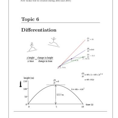
Mt6diffbook_feb2013 (1).pdf
June 2020 1
Degroot.pdf
June 2020 1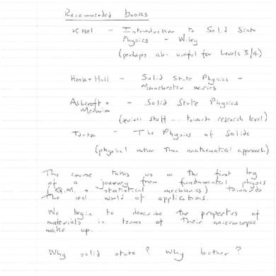
Charlton.pdf
June 2020 1
Qcd.pdf
June 2020 2
Gulf War Ii
May 2020 32